


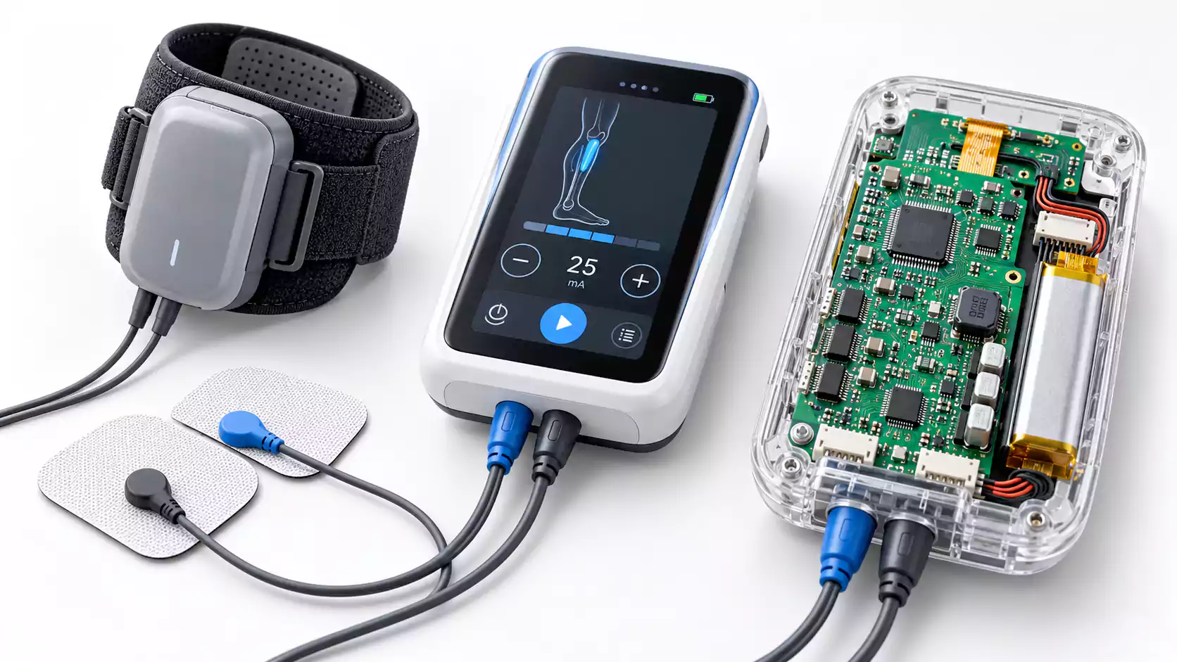

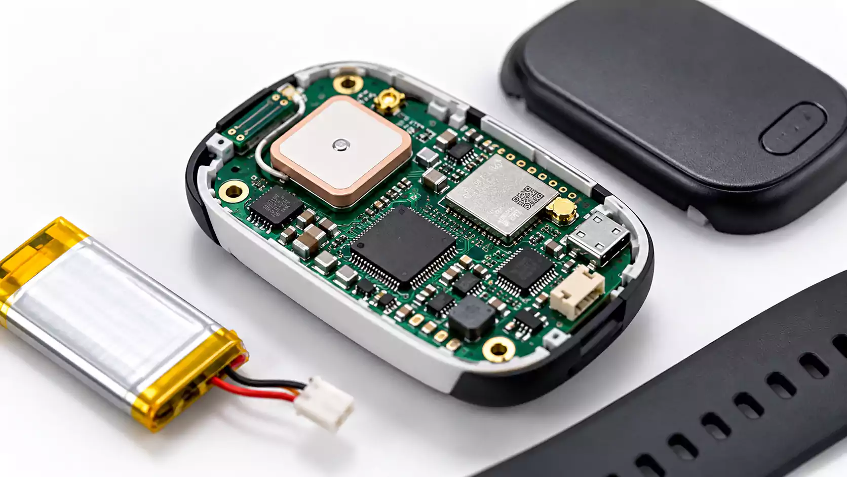

Choosing between IPC Class 2 and Class 3 affects PCB design tolerances, manufacturing requirements, inspection criteria, and long-term reliability.
Class 2 applies to dedicated-service electronics requiring reliable, extended operation. Class 3 is intended for high-performance electronics where continued operation or on-demand performance is critical.
The right choice depends on the product's failure consequences, operating environment, and applicable requirements. Understanding the technical differences helps engineers select appropriate design rules and avoid manufacturing or acceptance issues.
IPC Class 2 vs Class 3: Key Differences
| Requirement | IPC Class 2 | IPC Class 3 |
|---|---|---|
| Intended use | Dedicated-service electronics | High-performance, critical electronics |
| Reliability | Reliable, extended operation | Continued performance in critical applications |
| Annular ring | Certain controlled breakout conditions permitted | Stricter remaining-ring requirements |
| PTH copper plating | Class 2 thickness criteria | More stringent criteria for applicable structures |
| Plating voids | Limited defects may be acceptable | Tighter acceptance limits |
| Internal connections | Class 2 structural acceptance criteria | More restrictive structural requirements |
| Inspection | Class 2 acceptance criteria | Class 3 acceptance criteria |
| Cost | Generally lower | Potentially higher |
| Typical applications | Commercial and general industrial electronics | Critical medical, aerospace, and safety-related systems |
Specific dimensions and acceptance limits depend on the PCB construction and applicable IPC standard revision.
1. When Should You Choose IPC Class 3 Instead of Class 2?
The most important factor in choosing a class is what happens if the PCB fails.
Class 2 suits many electronic products that require dependable operation and can be serviced or replaced when needed.
Class 3 is more appropriate when a PCB failure could compromise safety, interrupt a critical function, or cause unacceptable operational consequences.
IPC Class Selection by Application
| Application | Class Selection Considerations |
|---|---|
| Industrial controllers | Class 2 for general control; Class 3 may be justified for critical functions |
| EV charging equipment | Depends on safety functions, operating conditions, and customer specifications |
| Automotive electronics | Depends on subsystem criticality and applicable automotive requirements |
| IoT gateways | Class 2 often suitable for serviceable or replaceable equipment |
| Medical devices | Depends on patient risk, intended use, and design requirements |
| Surgical robotics | Class 3 may be appropriate for critical control electronics |
| Aerospace electronics | Class 3 commonly specified with additional program requirements |
Does a Harsh Environment Require Class 3?
Environmental conditions alone do not determine IPC class.
For example, an outdoor industrial monitoring device may use Class 2 if the product's reliability requirements support that choice. An indoor, safety-critical controller may require Class 3 because failure could have serious consequences.
Also address temperature, vibration, humidity, and mechanical stress through material selection, PCB design, environmental protection, and appropriate qualification testing.
The final IPC class should match the product's approved engineering and contractual requirements.
2. IPC Class 2 vs Class 3: Technical Requirements
The main manufacturing differences involve annular ring integrity, plated-through-hole quality, internal connections, and acceptable defects.
Annular Ring and Drill Breakout
The annular ring is the copper surrounding a drilled hole.
Drilling and layer registration tolerances affect how much copper remains around the hole after manufacturing.
Class 2 allows limited breakout conditions, while Class 3 requires stricter control of the remaining annular ring.
The exact acceptance criteria depend on whether the feature is an internal or external annular ring and on the applicable hole structure.
Sufficient annular ring improves manufacturing margin and helps maintain reliable connections between copper layers.

Plated Through-Hole Copper Thickness
Plated-through holes (PTHs) electrically connect PCB layers through copper deposited along the hole wall.
Copper thickness is important because plated holes experience mechanical stress from thermal expansion and contraction.
Class 3 generally requires more stringent plating acceptance criteria for applicable hole structures.
The required thickness depends on the applicable IPC-6012F requirements, hole construction, and measurement criteria. Evaluate average plating thickness and local minimum thickness separately.
Reliable plated-through-hole manufacturing also depends on drilling accuracy, hole-wall preparation, and control of copper plating.
Plating Voids and Internal Defects
A plating void is an area where the intended copper deposit is missing or discontinuous.
Voids, internal layer separation, and other structural defects can reduce interconnection reliability, particularly under repeated thermal or mechanical stress.
Class 3 applies tighter acceptance criteria to relevant defects.
Laminate quality is also important. Delamination, resin-related defects, and internal connection integrity must meet the applicable acceptance requirements.
IPC Class 3 does not automatically require a different laminate material. Specify material properties such as Tg, thermal expansion, and dielectric performance based on the product's operating requirements.
3. PCB Design Rules and DFM Challenges for Class 3
A PCB designed for Class 2 may need adjustments to meet Class 3 acceptance criteria consistently.
The main challenge is maintaining sufficient manufacturing margin without unnecessarily increasing PCB size or routing complexity.
Annular Ring and Drill Registration
Drilling tolerances and layer registration affect the remaining annular ring.
Consider this simplified geometric example:
| Parameter | Value |
|---|---|
| Pad diameter | 0.55 mm |
| Nominal drill diameter | 0.30 mm |
| Nominal annular ring | 0.125 mm |
| Example drill offset | 0.075 mm |
| Approximate minimum remaining ring | 0.050 mm |
The nominal annular ring is calculated as:
Annular Ring = (Pad Diameter ? Drill Diameter) / 2
A drill offset reduces the copper remaining on one side of the hole.
This simplified example illustrates the effects of manufacturing tolerance. Actual IPC acceptance also considers hole dimensions, plating, registration, and the applicable inspection criteria.
Larger pads provide additional manufacturing margin but reduce routing space. As explained in PCB annular ring design, sufficient copper around drilled holes helps accommodate manufacturing tolerances. This trade-off matters most for HDI boards and fine-pitch BGA designs.
Class 3 DFM Checklist
Before releasing a Class 3 PCB design, engineers should review:
- Annular rings: Check remaining copper after drilling and registration tolerances.
- Pad and via dimensions: Confirm adequate manufacturing margin and routing clearance.
- Hole aspect ratios: Verify that the manufacturer can achieve the required plating quality.
- Layer registration: Review internal pad alignment and conductor-to-hole clearances.
- Materials and stackup: Match thermal and mechanical properties to the application.
- Fabrication data: Clearly define dimensions, tolerances, IPC class, and inspection requirements.
An early DFM review helps identify design constraints before production, improving yield and reducing rework risk.
4. Why Can a PCB Pass Electrical Testing but Fail Class 3 Inspection?
A PCB can pass electrical testing but still contain structural defects that fail Class 3 acceptance criteria.
Electrical testing verifies connectivity at the time of testing. Structural inspection evaluates manufacturing features that can affect long-term reliability.
This distinction matters in bare PCB quality verification: electrical testing confirms connectivity, while structural inspection evaluates plating quality and internal connections.
For example, a plated-through hole with a localized copper defect may still provide electrical continuity. Repeated thermal cycling can stress the remaining copper and potentially cause fatigue damage.
PCB Inspection Methods
| Inspection Method | What It Evaluates |
|---|---|
| Electrical testing | Opens, shorts, and electrical connectivity |
| AOI | Visible conductor-pattern defects |
| Microsection analysis | PTH copper thickness, plating voids, and internal connections |
| Thermal stress testing | Structural response to specified thermal exposure |
| Quality records | Compliance with agreed manufacturing and inspection requirements |
Microsection analysis is particularly useful because it reveals internal features that surface inspection cannot directly evaluate.
A cross-section can show variations in copper thickness, plating voids, laminate separation, and defects at internal connections. The IPC-A-600 acceptance criteria provide a framework for evaluating printed board characteristics against the specified class.
Inspection frequency, test coupons, sampling plans, and required records depend on the applicable standards and agreed quality requirements.
This explains why passing an electrical test does not automatically establish Class 3 conformity.

5. IPC Class 3 PCB Fabrication vs. PCB Assembly
Bare PCB fabrication and electronic assembly use different IPC standards.
| Standard | Main Purpose |
|---|---|
| IPC-6012 | Rigid PCB performance requirements |
| IPC-A-600 | Bare PCB acceptance criteria |
| IPC-A-610 | Electronic assembly acceptance criteria |
| J-STD-001 | Soldering process and artistry requirements |
Relevant IPC-6013 performance requirements cover flexible and rigid-flex PCBs.
One important distinction is between PTH copper plating and through-hole solder fill.
PTH copper plating is created during bare PCB manufacturing. Through-hole solder fill is evaluated after assembly, once component leads have been soldered.
These are separate manufacturing and acceptance requirements.
What If the Fabrication and Assembly Classes Differ?
A Class 3 bare PCB assembled and inspected to Class 2 requirements does not automatically qualify as a Class 3 electronic assembly.
Similarly, Class 3 assembly artistry cannot establish that an underlying Class 2 bare PCB meets Class 3 fabrication requirements.
For products requiring Class 3 performance, coordinate fabrication and assembly requirements before production.
6. IPC Class 2 vs Class 3: Cost, Yield & Lead Time
Class 3 manufacturing may involve additional process control, tighter acceptance criteria, and more demanding verification.
The cost and lead-time differences depend on PCB complexity, manufacturing capability, production volume, and customer requirements.
What Increases Class 3 PCB Cost?
- Manufacturing yield: Tighter acceptance requirements can increase rejection rates when the design has limited manufacturing margin.
- Plating control: Stricter plating criteria may require more process monitoring and verification.
- Inspection and documentation: Microsection analysis, testing, and specified quality records can add manufacturing costs.
- PCB complexity: High layer counts, fine-pitch routing, small vias, and tight registration tolerances can increase manufacturing difficulty.
Is Class 3 Worth the Additional Cost?
The decision should consider manufacturing cost alongside the potential consequences of failure.
For replaceable monitoring equipment, Class 2 may offer a good balance of reliability and cost.
For safety-critical or hard-to-service systems, stricter acceptance requirements may justify the added investment.
Early DFM review, realistic tolerances, and clearly defined inspection requirements help control Class 3 manufacturing costs and delivery risks.
7. How to Verify and Specify IPC Class 3 PCB Requirements
Evaluate a supplier's Class 3 manufacturing capability against the specific PCB requirements.
Supplier Verification Checklist
Before ordering, confirm:
- IPC standards: Applicable performance class and standard revisions.
- Manufacturing capability: Hole sizes, aspect ratios, plating, and layer registration.
- Inspection methods: How critical manufacturing characteristics are evaluated.
- Microsection reports: Applicable plating and structural inspection results.
- Electrical testing: Required test coverage and acceptance criteria.
- Traceability: Production lot identification and agreed quality records.
- Nonconformance control: Procedures for reporting and approving deviations.
A Certificate of Conformance (COC) documents the supplier's conformity declaration. Supporting inspection records provide additional evidence that the supplier evaluated the specified requirements.
Frequently Asked Questions
Is IPC Class 3 required for all medical or industrial PCBs?
No. The appropriate class depends on the product's function, failure consequences, reliability requirements, and customer specifications.
Is IPC Class 3 PCB manufacturing more expensive?
It can be. Costs depend on design complexity, manufacturing yield, inspection requirements, and documentation. There is no fixed Class 3 price premium.
Does a Class 3 PCB automatically mean Class 3 assembly?
No. PCB fabrication and assembly have separate acceptance requirements. Both must meet the applicable Class 3 specifications for the completed assembly to qualify.
Conclusion
Choosing between IPC Class 2 and Class 3 requires balancing product reliability, manufacturing feasibility, inspection requirements, and cost. Specify the appropriate class early, review critical design tolerances, and agree on acceptance criteria before production.
MULTIPCB provides multilayer PCB manufacturing, HDI, rigid-flex PCB, and PCB assembly services, with DFM review and quality-control support for demanding electronics projects.
