


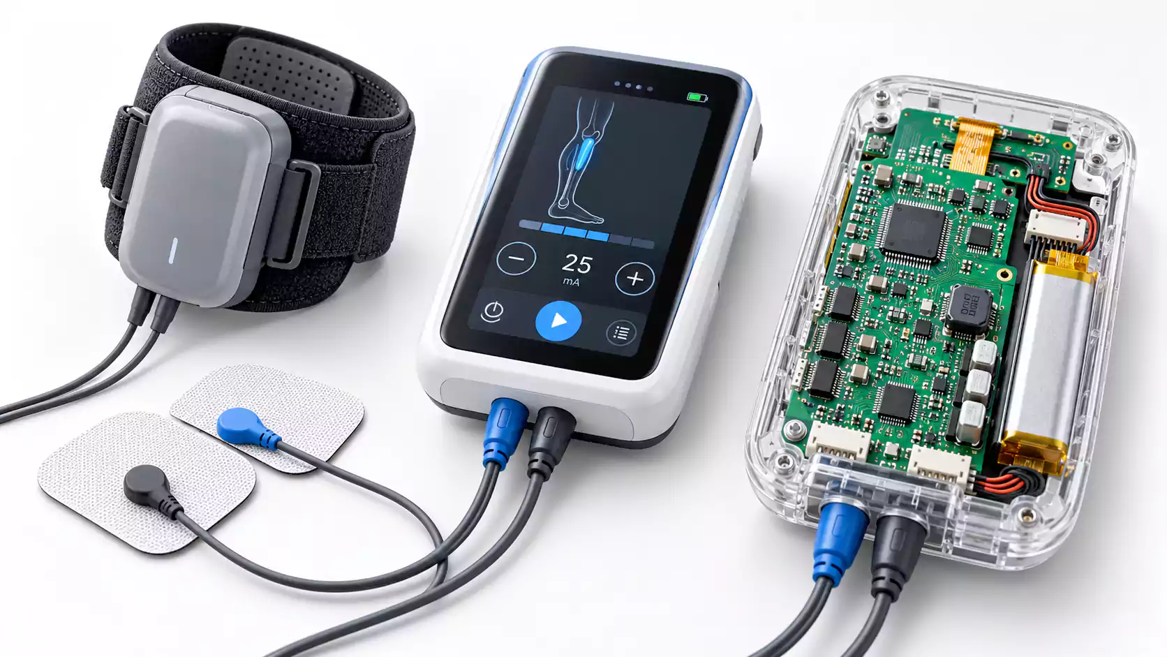

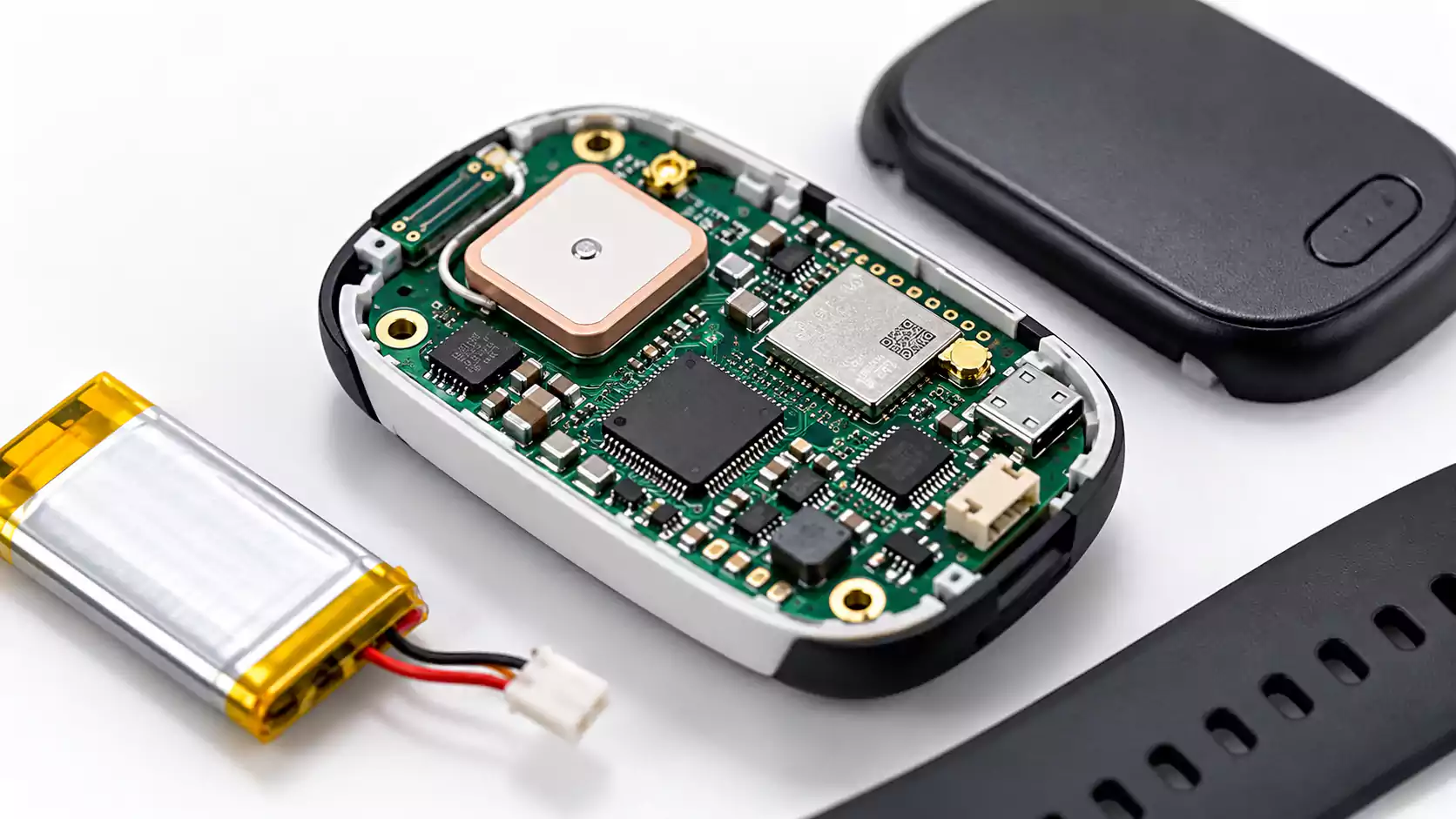

A multi-radio coexistence PCB integrates several wireless functions—such as Wi-Fi, Bluetooth, GNSS, and LoRa—on the same board. The main challenge is keeping one radio from degrading another when multiple transmitters and receivers operate close together.
Common problems include RF desense, antenna coupling, shared power noise, and receiver blocking. A practical way to analyze them is:
TX Aggressor → Coupling Path → RX Victim
Good multi-radio PCB design controls these paths through antenna placement, RF filtering, power and ground integrity, and concurrent-radio testing.
| Symptom | Likely Cause | First Check |
|---|---|---|
| GNSS performance drops during Wi-Fi TX | RF desense or conducted noise | Antenna isolation, GNSS power |
| Bluetooth degrades during Wi-Fi traffic | 2.4 GHz contention | PTA, channel planning |
| Sub-GHz range decreases | Blocking, harmonics, or power coupling | Filtering, antenna coupling |
| Radios work alone but degrade together | Multi-radio interaction | Concurrent TX/RX testing |
Why Radios on the Same PCB Interfere
Multi-radio interference can come from shared spectrum, unwanted RF energy, receiver blocking, and conducted noise through the PCB.

Same-Band Interference
Wi-Fi Bluetooth coexistence is a common example because both technologies use the 2.4 GHz ISM band. When both radios are active, packet loss, latency, and receiver blocking can increase.
Antenna isolation, channel planning, and coexistence control can work together to improve performance. In compact wireless products, wireless coexistence combines RF isolation with coordinated radio access when multiple wireless systems share spectrum.
Harmonics and Out-of-Band Energy
RF transmitters also generate energy outside their intended carrier frequency, including:
- Harmonics and spurious emissions
- Out-of-band noise
- PA broadband noise
- Clock and switching harmonics
These components can overlap with a nearby receiver band or raise the noise level seen by a sensitive RF front end.
| Aggressor | Main Interference to Check | Possible Victim |
|---|---|---|
| Wi-Fi / cellular TX | Out-of-band noise and spurs | GNSS or other receivers |
| Sub-GHz TX | Higher-order harmonics | Higher-frequency receivers |
| MCU / FPGA | Clock harmonics | GNSS / RF front end |
| DC/DC converter | Switching spectrum | Sensitive RF receivers |
RF Desense and Receiver Blocking
RF desense occurs when unwanted RF energy reduces receiver sensitivity.
A strong nearby transmitter can drive the receiver front end toward blocking or compression, even when the two radios operate in different frequency bands.
Strong TX → RF Front End → Blocking / Compression → Lower Sensitivity
This is one reason GNSS Wi-Fi interference can appear in a multi-radio system despite the large frequency separation between the two radios.
Power and Ground Coupling
Interference can also couple through the PCB power and ground network.
Shared regulators, common ground impedance, PA current bursts, DC/DC switching noise, and digital return currents can all carry noise into a sensitive receiver.
A well-designed RF coexistence PCB manages both radiated coupling and conducted noise across the board.
Build a Coexistence Matrix Before Layout
Before starting the PCB floorplan, map how each radio operates and which combinations may be active at the same time.
| Radio | Typical Band | Role | Receiver Sensitivity | Concurrent Operation |
|---|---|---|---|---|
| Wi-Fi | 2.4 / 5 / 6 GHz | TX/RX | Moderate | Often |
| Bluetooth | 2.4 GHz | TX/RX | Sensitive | Often |
| GNSS | L1/L5, etc. | RX | Very high | Usually |
| LoRa | Sub-GHz or 2.4 GHz | TX/RX | High | Application dependent |
For each radio pair, evaluate frequency overlap, harmonics, transmit power, receiver blocking tolerance, antenna isolation, filter rejection, and shared power or ground paths.
The main goal is to estimate how much interference may reach the victim receiver and how much isolation the system needs to maintain stable performance.
That isolation can come from several sources working together, including antenna separation, RF filtering, shielding, frequency planning, and time-domain coordination.
Antenna Placement and Isolation
Antenna placement is one of the earliest decisions in a multi-radio PCB floorplan. Position critical antennas before finalizing dense digital, memory, power, and connector sections.
Key Factors in Antenna Isolation
Multi-radio antenna placement depends on several factors:
- Physical separation
- Antenna orientation and polarization
- Radiation pattern
- Ground-plane geometry
- PCB-edge placement
- Battery and display location
- Enclosure materials
- Cable routing
The required spacing varies with the radio bands, antenna types, enclosure, and isolation target.
RF isolation also depends on the feed structure, matching network, stackup, and ground reference, so review the antenna feed network design alongside antenna placement.
Measure Isolation With S21
A practical development flow is:
Floorplan → Prototype VNA Measurement → Final Enclosure Validation
During prototype testing, measure antenna-to-antenna coupling with a VNA using S21, then compare the result with the system's isolation requirement.
Final validation should include the battery, display, enclosure, cables, and other nearby mechanical parts because these structures can affect antenna matching, coupling, and efficiency.
Wi-Fi and Bluetooth Coexistence
Wi-Fi and Bluetooth often share the 2.4 GHz band, so simultaneous activity can reduce throughput, increase latency, or raise packet error rates.
Many combo-radio platforms use Packet Traffic Arbitration (PTA) to coordinate radio access. A typical hardware interface uses signals such as:
REQUEST → PRIORITY → GRANT
Antenna isolation reduces direct RF coupling, while PTA coordinates radio access in time. Together, they improve coexistence when both radios operate in the same band.
On the PCB, coexistence control signals benefit from clean digital routing paths, good reference continuity, and clear separation from antenna and sensitive RF sections.
GNSS Desense: Protect the Most Sensitive Receiver
GNSS is often one of the most sensitive receivers on a multi-radio PCB. Typical signs of GNSS desense include lower C/N?, longer TTFF, fewer tracked satellites, and unstable fixes.
Common interference sources include Wi-Fi, cellular, and LoRa transmitters; DC/DC converters; high-speed processors; USB interfaces; and display circuitry.
A typical GNSS signal path may include:
Antenna → Protection → RF Filtering → LNA / Receiver
The exact topology depends on the GNSS chipset, antenna type, and RF reference design.
Key PCB considerations include:
- Keep the RF input path short and well referenced to a continuous ground plane.
- Provide clean, low-noise power for the GNSS receiver and LNA.
- Place switching regulators and high-speed digital circuits away from the GNSS antenna and RF front end.
- Use appropriate front-end filtering to reduce unwanted RF energy before it reaches the receiver.
- Maintain enough physical and electrical separation between the GNSS path and other active radios.
Together, these measures reduce radiated and conducted interference and help preserve GNSS sensitivity.
For systems combining multiple positioning technologies, our guide to UWB and GNSS PCB integration covers antenna placement, RF coexistence, power integrity, and GNSS interference in more detail.

RF Front-End Filtering
RF front-end filtering helps improve isolation between transmitters and sensitive receivers.
| Filter | Main Purpose |
|---|---|
| Low-pass | Reduce transmitter harmonics |
| Band-pass | Pass the desired receive band |
| Notch | Suppress a specific interfering frequency |
| SAW / BAW | Provide compact band-select filtering |
| Diplexer | Separate different RF bands |
Receiver-side filters need enough rejection to suppress nearby interference while keeping insertion loss low enough to preserve sensitivity.
A practical design balances:
Rejection ? Insertion Loss ? Receiver Sensitivity
For LoRa Wi-Fi coexistence, the main interference path depends on the operating band. Sub-GHz LoRa is more likely to interact with Wi-Fi through harmonics, receiver blocking, antenna coupling, or conducted noise. LoRa at 2.4 GHz overlaps directly with Wi-Fi, so channel planning and coexistence control become more important.
Power Integrity Is Part of RF Coexistence
Power integrity directly affects RF coexistence because transmitter current and switching noise can couple into sensitive receiver rails.
TX Current Bursts
Wi-Fi, LoRa, and cellular transmitters can draw fast current pulses during transmission. A stable PDN uses local energy storage, suitable bulk capacitance, short current paths, and low-impedance power distribution to keep supply rails steady.
Protect Sensitive RF Rails
GNSS receivers and LNAs benefit from clean, well-isolated power. Local regulation, ferrite beads, and properly selected decoupling can reduce conducted noise.
Component selection should consider impedance across the relevant frequency range, along with placement and return-path inductance.
Place DC/DC Converters Carefully
High-dv/dt switching nodes and high-di/dt current loops are major noise sources. Placing the converter and its hot loop away from the GNSS antenna, RF feed, LNA, and other sensitive receiver inputs helps reduce coupling at the source.
GNSS antenna → RF feed → LNA → receiver
Good power architecture and careful converter placement provide a cleaner RF environment for the entire multi-radio system.
RF Zoning, Grounding, and Shielding
A compact multi-radio PCB benefits from clear functional zoning:
GNSS | Wi-Fi/Bluetooth | LoRa/Cellular | Digital | Power
RF feed lines should use a continuous reference plane so return currents stay close to the signal path. Ground via fencing can improve isolation around RF sections, shield-can boundaries, and connector transitions.
Shield cans help reduce radiated coupling between sensitive receivers and noisy circuits. Their performance improves when the PCB also uses good antenna placement, clean power distribution, controlled return-current paths, and clear RF partitioning.
Effective RF isolation comes from combining these measures across the entire board.
Manufacturing and Assembly Tolerances
A multi-radio PCB should maintain stable RF performance from prototype through production.
Variations in trace width, dielectric thickness, Dk, copper thickness, etching, and solder mask can change controlled impedance and RF matching. For critical RF feeds, controlled impedance PCB design helps define stackup, trace geometry, and production tolerances before fabrication.
Small 0201 and 0402 RF components also introduce sensitivity to pad geometry, placement accuracy, solder volume, and component tolerances.
RF connectors and shield cans add another layer of variation, especially around grounding continuity and solder quality.
A robust design leaves enough coexistence margin to absorb normal production variations while keeping RF performance consistent across builds.
Validate Radios Under Concurrent Operation
Single-radio testing is not enough. Test a multi-radio design with the victim receiver active while another radio transmits under realistic operating conditions.
| Aggressor | Victim | Useful Metrics |
|---|---|---|
| Wi-Fi TX | GNSS RX | C/N?, TTFF, fix stability |
| LoRa TX | GNSS RX | C/N?, fix stability |
| Wi-Fi TX | Bluetooth RX | PER, throughput, latency |
| Bluetooth activity | Wi-Fi RX | Throughput, PER |
| MCU / DC/DC active | GNSS / LoRa RX | C/N?, SNR, sensitivity |
The failure pattern often reveals the coupling path. If GNSS performance drops during Wi-Fi transmission, check antenna isolation, GNSS power noise, and front-end filtering. Bluetooth issues during heavy Wi-Fi traffic often point to same-band contention and may benefit from channel planning or PTA.
If RF performance changes after you install the enclosure, recheck antenna matching and isolation in the final product. If production units show more variation than prototypes, review impedance consistency, RF component placement, soldering, and component tolerances.
Frequently Asked Questions
What is RF desense in a multi-radio PCB?
RF desense is reduced receiver sensitivity caused by nearby RF or conducted interference. Common sources include antenna coupling, harmonics, out-of-band emissions, and power noise.
Can Wi-Fi interfere with GNSS?
Yes. Wi-Fi can affect GNSS through RF coupling, receiver blocking, or conducted noise. Typical results include lower C/N?, longer TTFF, and less stable positioning.
Why do Wi-Fi and Bluetooth interfere with each other?
Both commonly operate in the 2.4 GHz band. Antenna isolation, channel planning, and Packet Traffic Arbitration (PTA) help improve coexistence.
How much antenna isolation is required?
It depends on transmit power, receiver tolerance, frequency separation, filtering, and antenna placement. Prototype S21 measurements are commonly used to verify antenna-to-antenna isolation.
How should multi-radio coexistence be tested?
Measure the receiver baseline, then repeat the test while another radio transmits. Compare metrics such as GNSS C/N? and TTFF, Wi-Fi throughput, Bluetooth PER, or LoRa SNR.
Conclusion
Reliable multi-radio coexistence PCB design requires control of frequency, space, power, ground, filtering, and operating timing.
A correct 50-ohm RF trace does not guarantee that Wi-Fi, Bluetooth, GNSS, LoRa, and other radios will operate reliably together. Evaluate the design as a complete system and test it with multiple radios active at the same time.
For multi-radio hardware moving from prototype to production, MULTIPCB supports controlled-impedance PCB fabrication, component sourcing, SMT assembly, and production-oriented DFM for RF and wireless electronics.
