


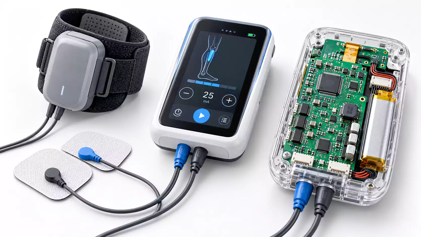

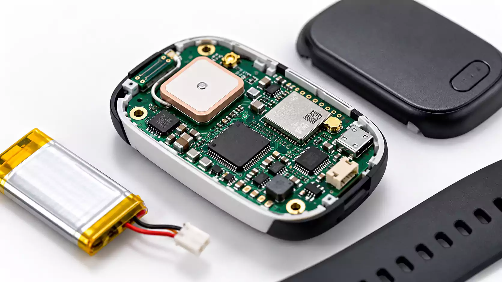

UWB GNSS PCB integration is becoming increasingly common in asset tracking, robotics, AGVs, industrial positioning, and other systems that need reliable indoor and outdoor location data.
The challenge is RF coexistence. GNSS receivers must detect extremely weak satellite signals while nearby UWB transmitters, DC/DC converters, MCU clocks, and digital interfaces operate. Poor antenna placement, noisy power rails, or uncontrolled RF routing can reduce GNSS C/N?, increase TTFF, and destabilize positioning.
A reliable design therefore depends on more than placing two radio modules on the same board. It requires careful antenna placement, controlled 50Ω routing, GNSS desense control, clean power and grounding, and production-ready RF validation.
This article focuses on those practical PCB design and manufacturing issues.

Why Combine UWB and GNSS?
GNSS and UWB solve different positioning problems.
GNSS works well outdoors with good satellite visibility, but performance can degrade indoors, near large structures, or in dense urban environments. UWB is better suited to local ranging and indoor positioning, making it useful in warehouses, factories, robotics, and asset-tracking systems.
A practical positioning device may therefore combine:
GNSS + UWB + MCU + IMU + Power + Wireless or Industrial Interfaces
Design the PCB as one integrated RF system rather than two independent radio modules.
GNSS Desense Is the Main Coexistence Risk
One of the most important problems in UWB and GNSS PCB design is GNSS receiver desensitization.
The GNSS module may still communicate normally with the MCU while its RF performance deteriorates. Common symptoms include lower C/N?, slower time first to fix, fewer tracked satellites, unstable positioning, or better GNSS performance when UWB is disabled.
| Symptom | Possible Cause |
| Lower GNSS C/N? | RF or broadband interference |
| Longer TTFF | Reduced receiver sensitivity |
| Fewer tracked satellites | GNSS front-end desense |
| Unstable position | Noise or antenna detuning |
| GNSS improves when UWB is off | RF, power, or ground coupling |
UWB and GNSS do not need to share the same operating frequency for interference to occur.
Noise can reach the GNSS receiver through several paths:
- Radiated coupling between antennas or nearby circuitry
- Conducted noise through shared power rails
- Shared ground impedance and return paths
- Clock harmonics and spurious emissions from digital circuits
For this reason, address RF coexistence during board floorplanning rather than after the prototype shows poor GNSS sensitivity.

UWB and GNSS Signal Chain Architecture
A clear signal-chain architecture makes PCB placement much easier.
GNSS front end
A passive GNSS path may look like:
GNSS Antenna → ESD → LNA / SAW Filter → GNSS Receiver
The exact order of the LNA and filter depends on the design goal. Placing the LNA earlier can help preserve noise performance, while filtering before amplification can improve tolerance to strong out-of-band signals.
An active GNSS antenna adds a DC bias path:
Active Antenna → RF Feed → ESD → Bias-T → GNSS Receiver
The bias network should follow the receiver or module manufacturer’s recommended architecture and should not introduce switching noise into the RF path.
UWB section
A typical UWB path is simpler:
UWB Antenna → Matching Network → UWB Transceiver
Both RF sections may share the MCU, IMU, memory, power system, and communication interfaces. These shared circuits are often important noise-coupling paths.
UWB and GNSS Antenna Placement
Decide antenna placement before detailed routing.
Consider the battery, enclosure, display, shield cans, cables, screws, and other metal parts, as they can change antenna impedance, efficiency, and radiation behavior.
UWB antenna
Follow the antenna or module manufacturer’s recommendations for:
- Board-edge position
- Copper keepout
- Ground boundary
- RF feed geometry
- Nearby component clearance
UWB ranging depends not only on impedance matching but also on antenna radiation and baseband behavior. The antenna can therefore affect ranging consistency even when return loss still looks acceptable.
GNSS antenna
Keep the GNSS antenna and front end away from switching regulators, inductors, high-current loops, MCU clocks, and fast digital buses.
GNSS patch and chip antennas also depend strongly on the surrounding ground plane and mechanical structure. Nearby batteries, metal parts, or displays can change antenna performance.
How far apart should UWB and GNSS antennas be?
There is no universal minimum spacing.
The practical approach is to maximize separation within the available mechanical space, preserve each antenna’s required keepout, and verify coexistence on the completed product.
Base final spacing on measured RF performance rather than a fixed-distance rule.
RF Feed and GNSS Front-End Layout
Both UWB and GNSS feedlines should be treated as controlled-impedance transmission lines. A well-designed antenna feed network must maintain impedance continuity through the transmission line, matching components, transitions, and antenna feed point.
A short 50Ω RF path with a continuous ground reference is generally preferred. For production boards, the trace geometry should be defined against the actual controlled impedance PCB stackup rather than a generic calculator value.
Pay particular attention to the complete RF transition.
| Area | Main Layout Concern |
| RF trace | Width, gap, and reference plane |
| Layer transition | Signal via and nearby return vias |
| U.FL / IPEX / SMA | Connector-to-PCB transition |
| Matching network | Pad parasitics and component placement |
| GNSS LNA | Short antenna-to-LNA path |
| ESD protection | Low parasitic capacitance |
A schematic label that says “50Ω” does not guarantee that the finished connector, pad, via, and trace transition will behave as a 50Ω structure.
Small RF matching components also deserve careful placement. At UWB frequencies, the pads, solder volume, spacing, and component position become part of the effective RF network.
Power, Grounding, and Digital Noise Control
In many positioning boards, the largest GNSS interference source is not the UWB carrier itself but the surrounding power and digital circuitry.
Power supply layout
Keep DC/DC switching nodes, inductors, and high di/dt loops away from the GNSS antenna and front end.
Place UWB decoupling capacitors close to the transceiver and keep the current loops short. Where necessary, sensitive GNSS rails can use additional filtering or a low-noise regulator.
Grounding
Avoid unnecessary ground-plane splits beneath RF traces.
A continuous reference plane generally provides a more predictable return path. Rely primarily on placement, return-path management, filtering, and physical separation to control noise.
Digital noise
Potential noise sources include:
MCU clocks, SPI, USB, Ethernet, memory buses, oscillators, and DC/DC harmonics.
Fast digital edges contain high-frequency energy even when the fundamental clock frequency is well below the RF band.
Via stitching and shield cans can improve isolation, but they cannot compensate for poor antenna placement or a noisy power architecture.
Manufacturing and SMT Can Change RF Performance
RF performance depends on the PCB that is actually manufactured, not only on the nominal CAD geometry. For UWB and GNSS hardware, consistent RF PCB manufacturing requires control of stackup, trace geometry, dielectric properties, etching, and impedance from prototype through production.
Controlled impedance is affected by:
trace width + copper thickness + dielectric thickness + Dk + plating + CPWG gap + solder mask
For a grounded coplanar waveguide, etching changes both the signal trace width and the spacing to the adjacent ground. Consistent process control is therefore important.
Solder mask is part of the RF structure.
At UWB frequencies, solder mask changes the dielectric environment around a transmission line.
The impedance model should match the intended production condition, including whether the RF trace is:
- Solder-mask covered
- Solder-mask open
Calculate the effect from the real stackup rather than estimate it using a fixed correction value.
Controlled-impedance tolerance
A ±10% tolerance is common for many controlled-impedance PCBs. Tighter limits such as ±5% may be specified when the RF design requires additional control.
The correct tolerance should come from the RF budget, not a generic UWB rule.
SMT assembly
Small matching networks are sensitive to assembly variation, which makes process control especially important during PCB assembly of UWB and GNSS RF sections.
For 0201 and 0402 components, pad geometry, component offset, solder volume, and spacing can affect parasitic inductance and capacitance.
For QFN or LGA RF devices, exposed pads, ground vias, and solder coverage should follow the component manufacturer’s recommendations.
U.FL connectors and shield frames also require consistent placement and soldering if RF performance must remain stable from prototype through production.
Test the Final Product, Not Just the Bare PCB
RF validation should continue after you install the PCB in the final mechanical assembly.
Test with the actual:
- Battery
- Enclosure
- Display
- Shield cans
- Cables
- Mounting hardware
- Nearby metal
For GNSS, useful measurements include:
C/N?, TTFF, satellites tracked, and fix stability
For UWB, evaluate:
ranging error, repeatability, packet reliability, and orientation sensitivity
One of the most useful coexistence tests is simply comparing system performance with UWB off and UWB on.
| Test | UWB Off | UWB On | What It Reveals |
| GNSS C/N? | Baseline | Compare | Receiver desense |
| TTFF | Baseline | Compare | Sensitivity degradation |
| Satellites tracked | Baseline | Compare | GNSS front-end impact |
| UWB ranging | Measure | Measure | Cross-system interaction |
| GNSS supply noise | Measure | Compare | Conducted coupling |
If GNSS performance changes significantly when UWB is enabled, tools such as a spectrum analyzer, near-field probe, oscilloscope, or clean external power source can help identify the dominant coupling path.
FAQ
Can UWB interfere with GNSS on the same PCB?
Yes. GNSS performance can degrade because of radiated coupling, power-rail noise, shared return paths, clock harmonics, or other broadband interference.
The most useful check is to compare GNSS C/N?, TTFF, and tracked satellites with UWB turned off and on.
How far apart should UWB and GNSS antennas be?
There is no universal minimum spacing.
Use the maximum practical separation, follow each antenna vendor’s keepout requirements, and verify performance in the final enclosure. Required spacing depends on antenna type, board size, ground geometry, enclosure, and GNSS front-end filtering.
Should UWB and GNSS use separate ground planes?
Usually not.
RF feedlines need a continuous reference plane for predictable impedance and return current. Isolation is generally better achieved through placement, filtering, controlled return paths, and shielding rather than arbitrary ground-plane splits.
From Prototype to Production
Reliable UWB GNSS PCB integration depends on the entire signal path, from antenna placement and RF routing to power integrity, PCB fabrication, SMT assembly, and final-product validation.
A practical development flow is:
RF architecture → antenna placement → controlled-impedance layout → coexistence testing → manufacturing control → production validation
MULTIPCB supports RF, GNSS, UWB, sensor, and industrial electronics projects with controlled-impedance PCB fabrication, component sourcing, PCBA, inspection, and prototype-to-volume production.
