




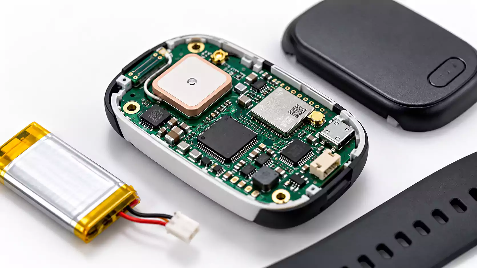

A photodiode transimpedance amplifier may look straightforward on a schematic, but its performance can change significantly once you implement it on a PCB.
In high-sensitivity optical systems, the photodiode current may be only a few nanoamps or picoamps. At these levels, PCB parasitic capacitance, surface leakage, flux residue, and nearby switching noise can directly affect measurement accuracy and stability.
Reliable Photodiode TIA PCB Design therefore depends not only on the op amp and feedback network, but also on how the high-impedance input is laid out and manufactured.
| Parasitic capacitance | Reduces phase margin and increases noise gain | Ringing or oscillation |
| Surface leakage | Adds unwanted input current | Offset and drift |
| Digital/power coupling | Injects noise into the summing node | Spikes or a higher noise floor |
For picoamp- and nanoamp-level signals, the PCB itself becomes part of the analog circuit.
Why Photodiode TIA PCBs Fail Even When the Schematic Is Correct
A photodiode TIA may be stable in simulation but behave differently once it is implemented on a real PCB.
The schematic usually shows only the main circuit elements: the photodiode, op amp, feedback resistor , and feedback capacitor . The PCB adds parasitic capacitance, leakage paths, and noise coupling that are not obvious in the ideal circuit.
| Ideal Circuit Element | Real PCB Adds |
|---|---|
| Photodiode | Pad and trace capacitance |
| Op amp | Package and via parasitics |
| Capacitance to nearby planes | |
| Ideal insulation | Surface and contamination-related leakage |
| No external coupling | Noise from switching circuits |
These non-ideal effects change the total input capacitance, leakage current, and noise the TIA sees. As a result, a circuit that appears stable in SPICE may show ringing, drift, or a higher noise floor after it becomes a physical Photodiode Amplifier PCB.

Define the High-Impedance Node First
Before routing the rest of the board, identify the TIA’s high-impedance summing node.
A typical signal chain is:
Photodiode → High-Impedance Summing Node → TIA → RC Filter / ADC Driver → ADC → MCU
The sensitive area usually includes the photodiode output, the trace to the op-amp inverting input, and the feedback junction.
Keep this region as small and isolated as practical. Unlike ordinary digital or low-impedance analog routing, extra copper, vias, test pads, and nearby switching signals can directly affect capacitance, leakage, and noise.
Photovoltaic vs. Photoconductive Operation
| Photodiode bias | Near 0 V | Reverse biased |
| Junction capacitance | Usually higher | Usually lower |
| Dark current | Lower | Higher |
| Speed | Lower | Higher |
| Main PCB concern | Leakage | Leakage and bias isolation |
For PCB layout, photodiode capacitance is especially important because it contributes directly to the total input capacitance that influences Photodiode TIA Stability.
Feedback Resistor : Gain Is Not Free
The basic transimpedance relationship is:
A larger feedback resistor produces more output voltage for a given photocurrent.
However, increasing also changes several other design parameters.
| Parameter | Effect of Increasing |
|---|---|
| Signal gain | Increases |
| Johnson noise | Increases |
| Bandwidth | Decreases |
| Leakage sensitivity | Increases |
| Sensitivity to PCB parasitics | Increases |
For this reason, select the feedback resistor as part of the complete signal chain rather than simply maximizing transimpedance gain.
TIA Feedback Capacitor and Photodiode TIA Stability
The TIA feedback capacitor helps maintain stability by compensating for capacitance at the op-amp inverting input.
A useful first-order model is:
As increases, phase margin can decrease, leading to:
overshoot → ringing → oscillation
First-Order Estimate
A common starting estimate is:
This is only a starting point. The final value depends on the actual op amp, total input capacitance, PCB parasitics, and required phase margin.
Why “Just Use 1 pF” Is Not a Design Method
If is too small, the TIA may ring or oscillate. If it is too large, bandwidth and response speed are reduced.
Verify the final value with the actual PCB and measured step response.
TIA Noise Sources and PCB Capacitance
A low-noise TIA Design requires control of both intrinsic circuit noise and PCB-induced effects.
| Noise Source / Mechanism | Main Effect | PCB Action |
|---|---|---|
| Feedback resistor thermal noise | Raises output noise floor | Avoid unnecessarily high |
| Input capacitance | Raises high-frequency noise gain | Minimize summing-node copper |
| Power-supply ripple | Conducted noise | Filter and isolate analog supply |
| MCU / clock / LED driver | Coupled noise | Increase physical separation |
| PCB leakage | Creates input-current error | Guarding and cleanliness |
PCB capacitance is not a thermal noise source itself.
Its importance comes from modifying noise gain, bandwidth, phase margin, and high-frequency peaking.
That is why Photodiode PCB Noise Reduction is often as much a layout problem as an op-amp-selection problem.
Transimpedance Amplifier PCB Layout: Six Critical Rules
This is where the schematic becomes a real TIA PCB layout.
1. Minimize Summing-Node Copper
Keep the photodiode-to-IN? connection as short and compact as possible. Less copper generally means lower capacitance, lower EMI pickup, and a smaller leakage surface.
2. Place RfR_f and CfC_f Directly Across the Feedback Path
Keep the feedback loop compact. Avoid unnecessary vias — they increase loop area and parasitic effects.
3. Keep the Photodiode Close to the Op Amp
Long traces between sensor and amplifier add capacitance and act as antennas for unwanted noise.
4. Keep Switching Nodes and Digital Clocks Away
Particular problem sources include DC/DC converters, MCU clocks, SPI edges, LED drivers, and laser drivers.
5. Place Decoupling at the Op-Amp Supply Pins
The goal is a short, low-inductance power-return loop.
6. Treat the Summing Node as a Special DFM Zone
Avoid unnecessary test pads, vias, exposed copper, routing underneath, and oversized pads. These features may seem harmless in ordinary PCB design, but they matter at high impedance.

Ground Plane Under the TIA: Where to Remove Copper
A continuous ground plane is usually beneficial — but the TIA summing node is a special case. A trace or pad directly above a ground plane forms a capacitor through the PCB dielectric, contributing directly to .
For a broader discussion of return paths and plane continuity, see our PCB ground plane design guide.
Where a local cutout makes sense
Remove reference-plane copper beneath the summing node and other capacitance-critical, high-impedance geometry. The goal is reducing unwanted trace-to-plane and pad-to-plane capacitance.
Where the ground plane should stay
| Area | Why Ground Should Remain |
|---|---|
| Power decoupling | Short current return |
| Op-amp output | Controlled low-impedance return |
| ADC-side circuitry | Stable reference path |
| Digital circuitry | Return-current control |
Photodiode Guard Ring PCB Design
A photodiode guard ring addresses a different problem than a plane cutout.
- A plane cutout primarily controls capacitance.
- A guard ring primarily controls surface leakage.

Guard Ring vs. Ground Shield
These are not the same technique. A guard is driven to a low-impedance voltage close to the sensitive node's potential, minimizing the voltage across any surface-leakage path — and therefore the leakage current itself.
Depending on the topology, the guard may be:
| Guard Type | Typical Use |
|---|---|
| Ground-referenced | Sensitive node near ground potential |
| -referenced | Single-supply biased TIA |
| Driven guard | Very high-impedance precision measurement |
The Guarding Trade-Off
Guarding isn't free. More copper around the sensitive node reduces leakage sensitivity but can increase capacitive coupling — trading lower leakage for lower bandwidth.
A high-speed photodiode TIA and a slow picoamp-level measurement circuit will typically call for different guarding strategies.
PCB Leakage Current and PCBA Cleanliness
When signal levels drop into the pA–nA range, PCB leakage current stops being a secondary effect and can directly limit measurement accuracy.
| Parameter | Value |
|---|---|
| Intended photodiode signal | 20 pA |
| PCB surface leakage | 5 pA |
| Resulting error | 25% |
Leakage Sources
Flux residue, moisture, dust, and other surface contamination can create parasitic leakage paths. Higher temperature and humidity can worsen the problem.
DFM for High-Impedance Nodes
Pad size, spacing, solder-mask openings, via placement, and high-value resistor footprints can all affect leakage. High-impedance zones therefore need different DFM priorities from standard digital circuitry.
These issues are especially important in high-impedance PCB design, where surface leakage and parasitic effects can directly influence measurement accuracy.
“No-Clean” Does Not Mean “Zero Leakage”
No-clean flux suits many products, but in pA- and nA-level designs, validate its electrical impact rather than assume it's negligible.
Verification Methods
| Method | What It Evaluates |
|---|---|
| ROSE | Ionic contamination |
| SIR | Surface insulation resistance |
| Dark TIA test | Actual board-level leakage and offset |
For high-impedance layouts, cleanliness is an electrical parameter — not just a manufacturing checkbox.
TIA Output to ADC
The TIA output typically connects to an ADC directly or through a small isolation network — an interface that can itself affect stability.
A SAR ADC, for instance, draws transient charge from its input during sampling. This kickback can disturb the amplifier's output.
A common architecture:
TIA Output → Series Resistor / RC Filter → ADC
The isolation network serves several purposes:
- Attenuates high-frequency noise
- Isolates ADC input capacitance from the amplifier
- Reduces sampling kickback
However, excessive filtering increases settling time. Size the network so the ADC input settles to the required accuracy before each conversion.
For high-resolution converters, ADC grounding, reference noise, and return-current control also become important; see our 24-bit ADC PCB layout guide for more detail.
Common Photodiode TIA PCB Failure Modes
| Symptom | Likely Cause | Possible PCBA Cause |
|---|---|---|
| Oscillation | Excess , poor phase margin | — |
| Ringing | too small or feedback loop too long | Component tolerance |
| High DC offset | Surface leakage or bias current | Flux residue |
| Humidity drift | Poor guarding | Ionic contamination |
| Noise when MCU runs | Digital coupling | — |
Two Useful Checks
Dark Leakage Test
Block the light input and measure offset and drift. This helps identify surface leakage and contamination.
Optical Step Response
Apply a controlled optical step and observe overshoot, ringing, and settling. This is one of the simplest ways to evaluate Photodiode TIA Stability.
FAQ
Should I place a ground plane under a photodiode TIA?
Avoid unnecessary ground-plane copper directly beneath a capacitance-sensitive summing node. A local cutout can reduce parasitic capacitance, but keep the ground plane intact where low-impedance return paths require it.
How do I choose the TIA feedback capacitor?
Estimate from the total input capacitance, feedback resistance, and op-amp bandwidth, then verify the value with the actual PCB and measured step response.
Where should a photodiode guard ring be connected?
The guard should be held at a low-impedance voltage close to the sensitive node potential. Depending on the circuit, this may be ground, , or a driven guard.
How does PCB leakage current affect a photodiode amplifier?
PCB leakage acts like an unwanted input current. In picoamp- and nanoamp-level circuits, even small surface leakage can create significant offset and drift.
Conclusion
Reliable Photodiode TIA PCB Design depends on more than the op amp itself.
Key PCB-level controls include minimizing summing-node capacitance, keeping the feedback network compact, using local plane cutouts where needed, controlling leakage with appropriate guarding, isolating switching noise, and maintaining good PCBA cleanliness.
For photodiode amplifiers and other high-impedance sensor electronics, MULTIPCB provides PCB fabrication and PCBA support, including DFM review, assembly, and testing for sensitive analog designs.
