


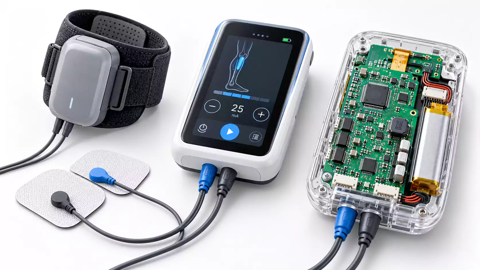

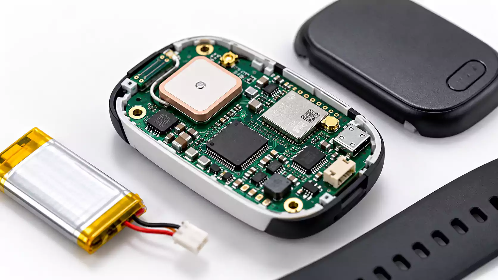
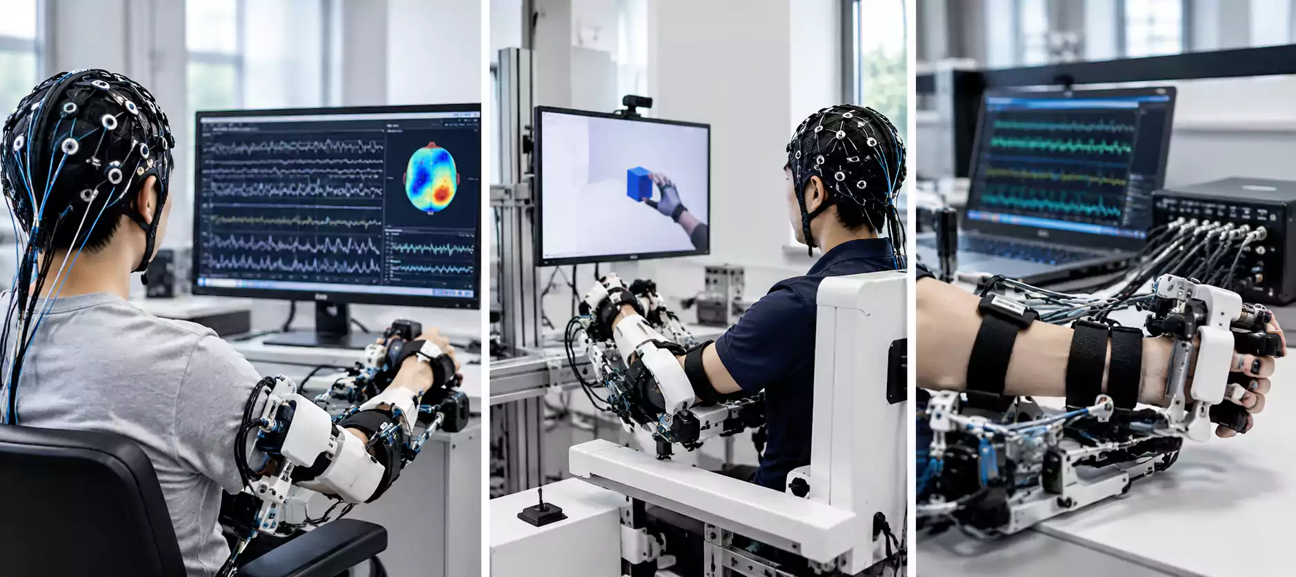
Neural Interface PCB Design is challenging because extremely small biological signals must coexist with ADCs, processors, power converters, communication interfaces, and sometimes stimulation circuitry.
A typical recording path is:
Neural Electrode / MEA → Input Protection → Low-Noise AFE → ADC → MCU / FPGA → Communication
For bidirectional systems, a stimulation path is added:
Stimulator / Current Driver → Neural Electrode
The PCB must preserve weak neural signals while controlling leakage, digital noise, channel crosstalk, stimulation artifacts, and manufacturing variation.

Neural Interface PCB Architecture
Neural interfaces may acquire EEG, ECoG, local field potentials, or action potentials. Compared with conventional EEG and ECG PCB design, high-channel-count neural systems place greater demands on electrode routing, synchronization, and stimulation isolation.
These signals differ in amplitude and bandwidth, which affects AFE bandwidth, filtering, ADC sampling rate, and noise requirements.
Electrode impedance is equally important. The recording front end should present sufficiently high input impedance so it does not significantly load the electrode.
Channel count also changes the hardware architecture.
| Channel Count | Typical Architecture | Main PCB Challenge |
|---|---|---|
| 8–32 | Multichannel AFE + MCU | Low-noise analog layout |
| 64–256 | Multiple AFEs + MCU/FPGA | Synchronization and crosstalk |
| 512+ | ASIC/AFE arrays + FPGA + HDI | Dense fan-out and data bandwidth |
A high-channel-count neural interface PCB is therefore not simply a larger version of an 8-channel acquisition board.
Keep the Electrode-to-AFE Path Short
The most sensitive section of the board is usually:
Electrode Connector → Protection / Filter → AFE
High-impedance input traces should be kept short because long routes increase exposure to:
- capacitive pickup,
- 50/60 Hz interference,
- digital switching noise,
- parasitic capacitance,
- surface leakage.
The first amplification stage should therefore be placed close to the electrode connector whenever the system architecture allows it.
Input Protection Requires Trade-Offs
Protection devices can affect signal quality.
A component with excessive leakage may disturb a high-impedance input, while excessive capacitance can change the input response. Input protection should therefore be designed as part of the analog signal chain rather than added after the circuit is finished.
Important parameters include:
- leakage current,
- junction capacitance,
- series resistance,
- input filter bandwidth,
- electrode impedance.
Guard traces may help around very high-impedance nodes, but they do not compensate for poor PCB cleanliness. Effective leakage control and guard-ring layout should also account for humidity, contamination, and the electrical environment around the protected input.
Devices such as the ADS1299 low-noise biopotential ADC integrate multichannel amplification and high-resolution conversion, but PCB layout still determines how much of that performance can be preserved in the final system.
Grounding and Digital Noise Control
A common mistake is automatically splitting analog and digital ground.
In many neural recording systems, a continuous reference plane combined with careful component placement provides better return-current control than arbitrary ground-plane cuts.
The goal is to keep noisy current loops away from the neural front end.
Separate Functional Zones
A practical board can be divided into three areas.
Quiet Analog Zone
- electrode inputs,
- AFE,
- ADC,
- voltage reference,
- low-noise analog power.
Digital Zone
- MCU,
- FPGA,
- memory,
- SPI,
- USB,
- Ethernet,
- wireless interfaces.
Power Zone
- DC/DC converters,
- inductors,
- high-current switching paths.
High-speed clocks and digital buses should not cross sensitive analog input areas. Their return currents should remain local to the digital region.
The same principle applies to SPI, USB, Ethernet, and FPGA interfaces: physical separation matters as much as schematic separation.
Power and Thermal Design
A 24-bit converter or low-noise AFE cannot perform well if its power rails and voltage reference are noisy.
A practical power architecture may use:
Battery / Input Power → DC/DC → Filter / LDO → AFE / ADC
Keep the switching converter away from electrode inputs and analog reference circuitry, and keep its high-current switching loop compact.
Key power-integrity concerns include:
- DC/DC switching ripple,
- ADC reference noise,
- analog rail noise,
- load transients,
- ground impedance,
- decoupling placement.
A high-resolution ADC does not guarantee high-resolution measurement. The entire signal chain determines the actual noise floor and usable resolution.
High Channel Count Also Creates Heat
As channel count increases, multiple AFEs, ADCs, FPGAs, and communication devices can create localized heating.
Thermal gradients can affect precision analog performance and may also matter in wearable or implantable hardware.
Consider:
- heat-producing component placement,
- copper distribution,
- thermal vias,
- FPGA heat spreading,
- temperature-sensitive analog components.
Multi-Channel Neural Recording
Scaling from dozens to hundreds of channels introduces two major challenges: crosstalk and data bandwidth.
Channel-to-Channel Crosstalk
Crosstalk can result from:
- adjacent high-impedance traces,
- shared reference impedance,
- clock coupling,
- noisy power rails,
- connector pin assignment,
- stimulation routing.
Channels do not need to be geometrically identical, but they should operate in similar electrical environments.
Estimate Data Bandwidth Early
A simple estimate is:
Raw Data Rate ≈ Channels × Sampling Rate × Bits per Sample
For example:
128 channels × 30 kS/s × 24 bits ≈ 92 Mb/s
before protocol overhead.
At higher channel counts, this can push the system from a simple MCU toward FPGA-based aggregation and faster data links.
Recent high-density neural-interface research demonstrates how channel scaling can lead to architectures that combine custom ASICs, routing or interposer boards, FPGA aggregation, and high-bandwidth data links.
When HDI Becomes Necessary
High-channel-count systems quickly run out of routing space.
HDI PCB technology may become necessary when neural systems use:
- fine-pitch BGAs,
- dense AFE arrays,
- microelectrode arrays,
- microvias,
- via-in-pad,
- fine-line routing,
- interposer boards.
Microelectrode arrays may also require FPC tails, rigid-flex structures, or dense board-to-board connectors.
The PCB fabricator should be involved before routing is finalized.
If line/space, microvia size, capture pads, registration tolerance, and flex construction are reviewed only after layout is complete, a major redesign may be required.
Recording and Stimulation on the Same PCB
This is one of the most difficult neural-interface design problems.
The recording path may be measuring microvolt-level neural signals while the stimulation path delivers a much larger voltage or current pulse.
That stimulation energy can couple into recording channels through:
- the electrode interface,
- tissue,
- PCB capacitance,
- shared return paths,
- power rails,
- connectors.
The result is a stimulation artifact that may saturate the AFE.

AFE Saturation and Recovery
Artifact amplitude is only part of the problem.
If the amplifier saturates, the system must recover quickly enough to observe neural activity after the stimulation pulse.
Important considerations include:
- amplifier input range,
- gain,
- stimulation amplitude,
- recovery time,
- blanking interval,
- input switching.
PCB Isolation Matters
Recording and stimulation paths should not share long parallel routes or uncontrolled return paths.
Consider separating:
- recording inputs,
- stimulation outputs,
- power domains,
- return-current paths,
- connector pins.
Depending on the architecture, artifact mitigation may also use hardware blanking, temporary input isolation, gain control, or digital artifact processing.
A useful validation test is to inject a known stimulation waveform and measure both adjacent-channel saturation and recovery time.
Surface Leakage and PCBA Cleaning
For high-impedance neural inputs, PCB cleanliness directly affects electrical performance.
Flux residue, moisture, and ionic contamination can create leakage paths between nodes.
Possible symptoms include:
- offset drift,
- elevated noise,
- humidity-dependent errors,
- unstable high-impedance channels.
This is why the assembly process matters as much as the schematic.
Cleaning Should Be Defined Before Production
“No-clean” flux does not mean every high-impedance neural interface can be assembled without cleaning.
The correct process depends on:
- input impedance,
- board geometry,
- flux chemistry,
- humidity exposure,
- coating requirements,
- validated leakage limits.
Fine-pitch neural interface assemblies may also contain QFNs, BGAs, FPC connectors, microvias, and via-in-pad structures.
AOI and X-ray can identify many assembly defects, but they cannot confirm low-noise analog performance.
Functional Testing for Neural Interface PCBA
A neural interface PCBA should be tested for analog performance, not just continuity.
| Test | What It Verifies |
|---|---|
| Known-input signal | Gain and offset |
| Noise-floor test | Analog noise |
| Crosstalk test | Channel isolation |
| Stimulation waveform test | Pulse accuracy |
| Artifact-recovery test | Recording/stimulation recovery |
For multi-channel boards, automated fixtures can compare channels quickly and identify abnormal variation.
Neural Interface PCB Design Checklist
| Item | Key Question |
|---|---|
| Signal | What amplitude and bandwidth must be recorded? |
| Electrode | What impedance range is expected? |
| Channels | How many channels must the PCB support? |
| Stimulation | What voltage/current and pulse conditions are required? |
| Interconnect | FPC, MEA, or board-to-board connector? |
| PCB | Is HDI, microvia, or via-in-pad required? |
| Cleaning | What leakage and contamination limits apply? |
| Testing | What noise, crosstalk, and recovery limits must be verified? |
Higher channel counts may require HDI, while high-impedance inputs demand tighter leakage and cleanliness control. Define these requirements before layout and DFM review.
Conclusion
Reliable Neural Interface PCB Design requires careful control of low-level signal paths, channel density, stimulation interference, and surface leakage throughout both design and manufacturing.
Keep electrode-to-AFE paths short, isolate noisy digital and stimulation circuits, plan high-channel-count routing early, and verify analog performance with functional testing.
For neural recording, BCI, and neurostimulation projects, MULTIPCB provides PCB fabrication, PCBA, DFM review, inspection, and prototype-to-production support.
