


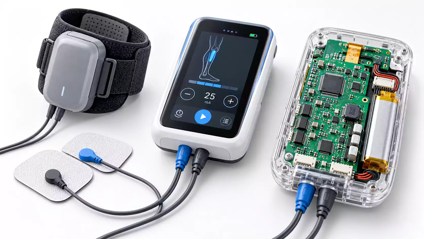

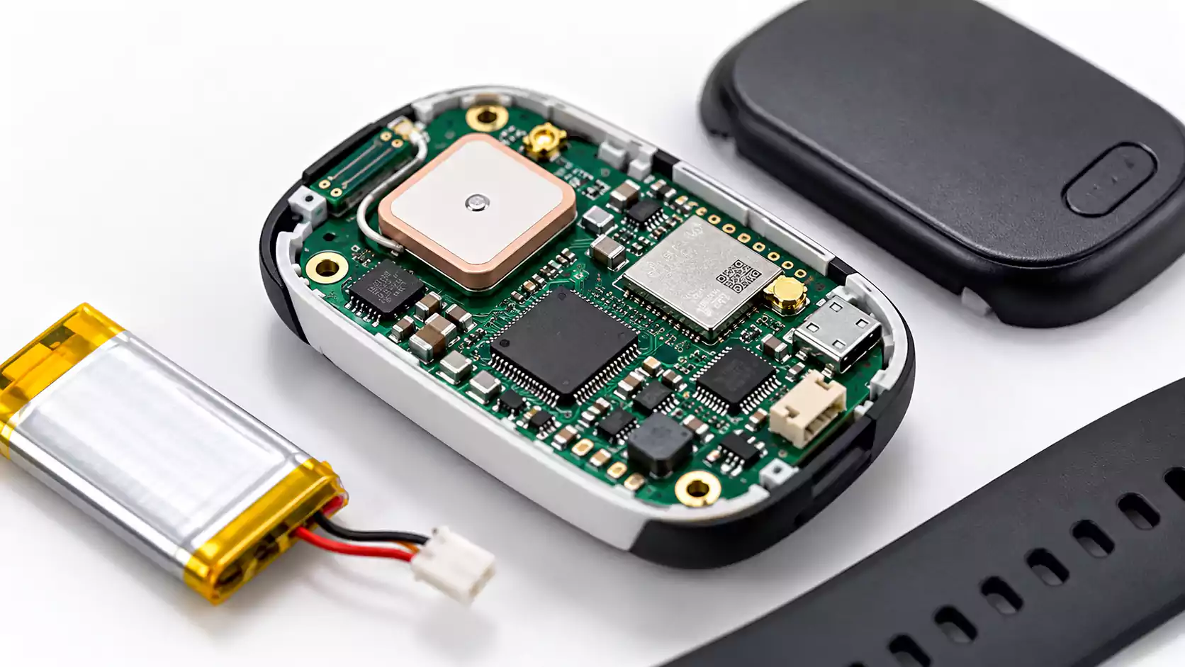

Designing an EEG or ECG PCB is a different discipline from laying out a conventional digital control board. These systems capture very small biopotential signals, often on the same board as ADCs, microcontrollers, clocks, switching regulators, USB interfaces, and wireless radios.
A board can power up correctly, communicate over SPI, and stream ADC data—and still produce an unusable waveform. The culprit is usually 50/60 Hz interference, baseline drift, digital coupling, surface leakage, or unstable grounding.
Good EEG and ECG PCB design accounts for the full signal path: electrode connector, analog front end, ADC, power system, and digital interface, plus fabrication, medical PCB assembly, cleanliness, and functional testing.
1. Why EEG and ECG Boards Are Different
EEG and ECG systems both measure biopotential signals, but their requirements diverge:
| Channel count | Typically many (8–256+) | Few (1–12 typical) |
| Signal amplitude | Very small — ?V range | Larger — mV range |
| Primary layout challenge | Ultra-low noise, channel-to-channel matching | Input impedance, CMRR, patient-interface design |
The challenge isn’t just signal amplitude. A low-noise medical PCB has to guard against:
- capacitive or inductive noise coupling
- uncontrolled return-current paths
- leakage across high-impedance input nodes
- switching and digital power noise
- channel-to-channel mismatch
An EEG acquisition board can function perfectly on the digital side and still fail as a measurement instrument—a clean SPI waveform says nothing about the analog path's cleanliness.
2. Signal Chain for a Biopotential Acquisition Board

A typical signal chain looks like this:
Electrode → Input Protection → RC/EMI Filter → Analog Front End → ADC → MCU → USB/BLE/Wireless Interface
Devices like the ADS1299 integrate much of the signal conditioning and conversion, but the surrounding PCB still determines whether that integration pays off.
Electrode inputs and protection. The electrode interface is high-impedance and noise-sensitive. Judge input protection not just on ESD robustness, but on leakage current, parasitic capacitance, and symmetry. Mismatched protection or filter components ahead of the amplifier will degrade common-mode rejection before the signal is even amplified. For differential channels, keep both sides of the input network symmetric — placement, trace geometry, and parasitic capacitance should mirror each other as closely as practical.
BIAS and RLD. EEG systems typically use a patient bias circuit; ECG systems use right-leg drive (RLD). The implementation differs, but the goal is the same: manage the patient’s common-mode voltage and suppress interference. Treat this path as core measurement circuitry, not an optional add-on. Keep feedback components close to the AFE, and route the BIAS/RLD output away from fast digital signals and switching nodes.
3. Floorplanning for Low-Noise Layout
Good EEG PCB layout starts with the signal path, not the microcontroller. A sensible placement order is:
Electrode Connector → Protection → AFE/ADC → Digital Interface
This keeps sensitive input circuitry compact, rather than squeezed into whatever space is left after the digital section is placed.
Divide the board into functional zones:
- high-impedance electrode input
- analog front end and ADC
- clean analog power
- digital processor and communication
- switching power
- RF/wireless
The point isn’t to draw arbitrary boundaries — it’s to control where noise currents flow.
Switching regulators need particular care. Keep the switching node, power inductor, input capacitor loop, and other high di/dt paths away from the AFE. A DC/DC converter can work fine in an EEG or ECG product as long as its high-frequency current loops are localized and don’t share return paths with sensitive circuitry. The same logic applies to oscillators, SPI clocks, USB, BLE, and Wi-Fi: none of it is inherently incompatible with biopotential sensing; it just belongs in the noisy digital section.

4. Grounding and Isolation Strategy
Grounding is critical in EEG/ECG PCB design. Instead of automatically splitting AGND and DGND, start with functional partitioning and control return currents. For many compact mixed-signal boards, a continuous ground plane is preferable because an unnecessary split can force return currents onto longer paths and increase noise coupling.
The key question is not whether a trace is analog or digital, but where its return current flows. Fast clock or digital traces should not cross sensitive analog regions.
A net tie is only needed when analog and digital grounds are intentionally kept as separate nets and must connect at a defined point; it is not a mandatory ADS1299 layout rule.
If the board connects to USB, a charger, mains-powered equipment, or other external interfaces, consider the isolation boundary, creepage, clearance, and isolated power architecture at the system level.
5. ADS1299 Layout Guidelines
The ADS1299 is widely used in multichannel EEG systems, and its PCB layout directly affects noise performance.
Analog inputs. Keep INxP/INxN traces short, balanced, and away from digital signals. Place matched RC input components close to the device, and treat SRB1/SRB2 as sensitive shared analog paths.
Reference and decoupling. Place reference, VCAP, and supply capacitors close to their pins with short return paths. Avoid routing these loops through noisy digital or switching regions.
Power and digital routing. Follow the ADS1299 datasheet for analog, digital, and charge-pump supply connections. Keep SCLK, DIN, DOUT, DRDY, and CLK away from electrode inputs and reference circuitry.
A 2-layer board can work for simple prototypes, but a 4-layer PCB usually provides better ground referencing, power routing, and multichannel layout flexibility.
6. Leakage, Guarding, and PCB Cleanliness
High-impedance medical boards are sensitive to surface leakage and electromagnetic noise. Leakage paths can come from flux residue, ionic contamination, moisture, fingerprints, contaminated connectors, PCB surface damage, or leakage through protection devices — which is why surface contamination on a medical PCB is an electrical problem, not just a cosmetic one.
Guard traces help in some high-impedance applications, but “put ground around the input” isn’t a universal fix. A grounded guard and a driven guard behave differently, and for very sensitive nodes the guard potential may need to track the signal more closely to reduce leakage.
Solder mask deserves the same scrutiny. Removing mask around a high-impedance node isn’t automatically an improvement — cleaning accessibility, contamination risk, exposed laminate, environmental exposure, and manufacturing robustness all factor in.
Leakage and noise paths aren’t confined to the PCB, either. Connectors and cables can introduce their own problems, especially in multichannel EEG systems.
7. 50/60 Hz Noise, Power, and EMC
How interference gets in
Mains interference can enter the system through several routes: the patient's body picks up common-mode interference, electrode impedance mismatch converts some of that into a differential signal, cables act as antennas, and PCB asymmetry further erodes common-mode rejection. In other words, CMRR is decided before the signal ever reaches the amplifier — even an AFE with excellent datasheet CMRR can underperform at the system level if input resistors, capacitors, protection devices, or electrode impedances are mismatched.
Power architecture
An LDO isn't automatically better than a DC/DC converter — a battery-powered design may need switching regulation for efficiency. The real objective is controlling switching frequency, harmonics, hot-loop geometry, placement, and post-regulation filtering.
Shielding
Shielding is a supporting measure, not a fix. It can reduce radiated coupling, but it won't compensate for a poor return-current path or an asymmetric input network.
8. From Layout to Repeatable PCBA Manufacturing
A working prototype doesn't automatically translate into repeatable medical device PCB assembly.
Component tolerance and matching
Tolerance and matching matter in input filters, gain networks, and reference circuits. If a production channel ends up with components at opposite ends of their tolerance range, channel consistency or CMRR can shift even though every part is technically within spec.
Assembly cleanliness
Flux chemistry, cleaning, drying, handling, and rework all need control around high-impedance areas. Rework in particular deserves attention — extra flux and localized heat can change analog performance even after the original defect is fixed.
Setting cleanliness acceptance criteria
For medical PCB manufacturing, cleanliness acceptance criteria should be based on the specified process, materials, product risk, and validated manufacturing controls — not a single generic contamination number pulled from an unrelated product.
9. What Production Testing Should Actually Verify
SPI checks, AOI, and X-ray are useful, but none of them can tell you whether an EEG channel has an acceptable noise floor. A solid test strategy separates assembly verification from analog performance verification:
| Shorted-input noise screening | Channel RMS noise under a controlled input condition | Compare against validated production limits |
| Precision waveform injection | Channel gain and basic signal-path operation | Use a calibrated source or patient simulator; full CMRR characterization is better suited to engineering validation |
| Digital interface verification | SPI, USB, BLE, sampling continuity, packet integrity | Confirms both the analog and digital sides of the assembly |
The principle is simple: a visually perfect EEG or ECG PCBA can still be electrically unusable.
10. Common Failures and a Release Checklist
| Symptom | Likely Cause | First Check |
| Strong 50/60 Hz hum | Poor common-mode rejection | Input balance and grounding |
| Periodic spikes | DC/DC or clock coupling | Switching and clock placement |
| Baseline drift | Leakage or contamination | High-impedance input area |
| One noisy channel | Routing or component mismatch | Compare channel layouts |
| Waveform shifts with BLE activity | RF coupling | Antenna and return paths |
| Touching the PCB changes the signal | Leakage or shielding issue | Input nodes, surface cleanliness |
| ADC saturation | Excess offset or common-mode voltage | Electrode and BIAS path |
| Prototype works, batch doesn’t | Process variation | Cleaning, BOM, rework |
Before production, verify that the electrode-to-AFE path is short, differential inputs are balanced, return-current paths are controlled, ADS1299 decoupling follows the datasheet, and sensitive analog areas are kept away from noisy digital and power circuits.
FAQ
1. Should AGND and DGND be separated on an ADS1299 PCB?
Not always. Start with functional partitioning and controlled return paths. Split grounds only when the system architecture requires separate ground domains.
2. Can ADS1299 be used on a 2-layer PCB?
Yes. However, a 4-layer PCB generally provides better ground referencing, power routing, and multichannel layout flexibility.
3. How can 50/60 Hz noise be reduced in an EEG or ECG PCB?
Focus on balanced electrode inputs, matched RC networks, controlled grounding, cable shielding, low-noise power, and separation from digital or switching circuits.
4. Why is PCB cleanliness important for EEG and ECG circuits?
High-impedance inputs are sensitive to surface leakage. Flux residue, moisture, and contamination can cause baseline drift and unstable measurements.
Conclusion
EEG and ECG boards are precision measurement systems. Signal-chain design, grounding, leakage control, power integrity, assembly cleanliness, and functional testing all directly affect signal quality.
For EEG and ECG projects requiring PCB fabrication, component sourcing, and medical PCBA assembly, MULTIPCB supports development from prototype through volume production.
