




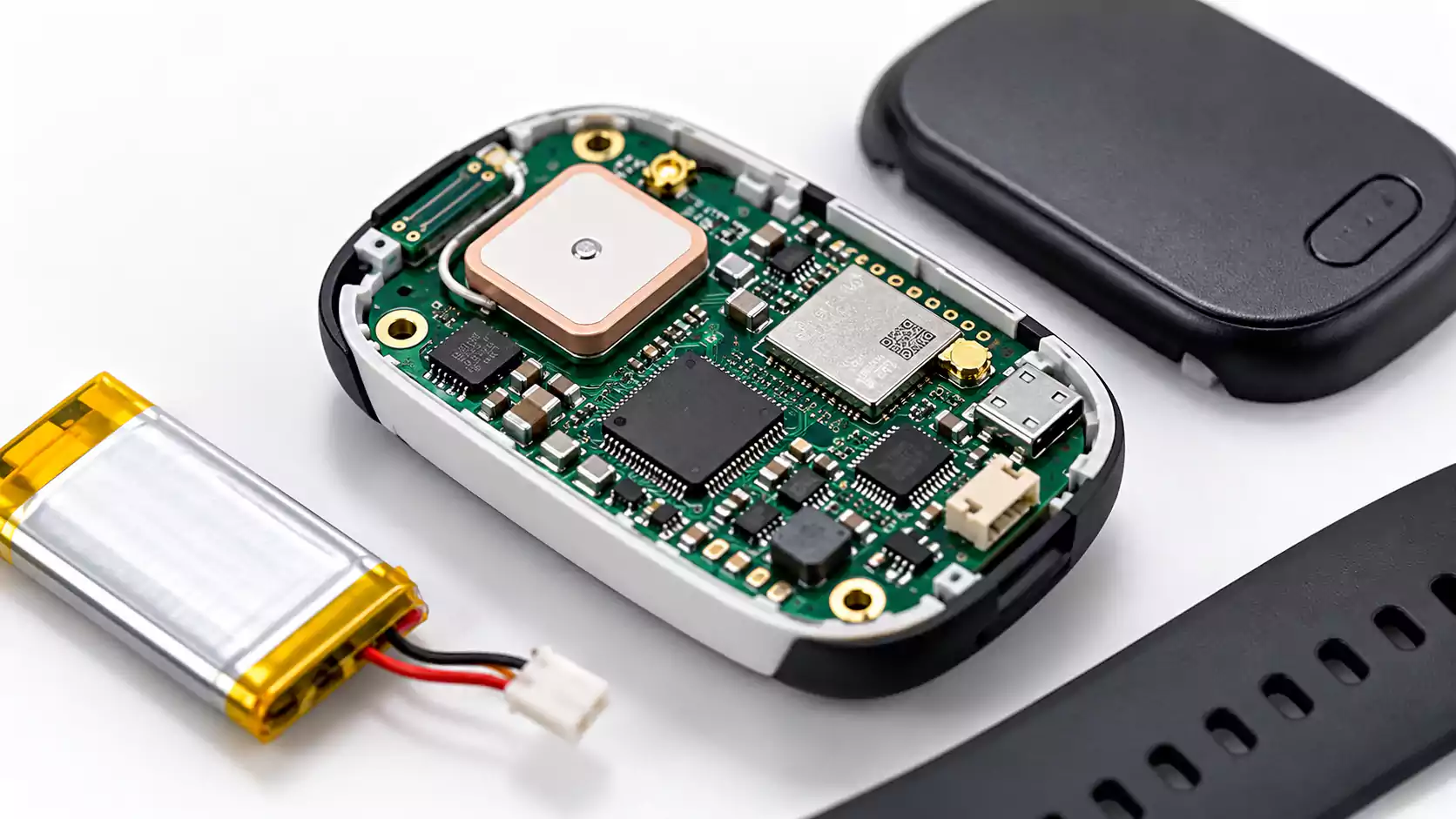
Industrial monitoring systems often use several connected PCBs, with each board handling a specific function. A typical architecture includes:
Sensor Board → CPU Board → Interface Board
This structure is common in gas detection, process control, condition monitoring, environmental sensing, and industrial instrumentation. It allows each board to be optimized for measurement accuracy, computing, communication, mechanical placement, and field reliability.
Successful multi-board PCB design depends on how these boards work together. Even when every PCBA operates correctly on the bench, the complete system can still experience connector misalignment, ADC noise, power-distribution issues, EMI, or inaccessible test points after assembly.
For an industrial monitoring PCB system, you must consider architecture, electrical interfaces, mechanical fit, grounding, assembly, and system-level testing.
Why Industrial Monitoring Systems Use Multiple PCBs

Different parts of an industrial monitoring system have very different requirements.
| Board | Typical Functions | Main Design Priority |
| Sensor Board | Sensor excitation, AFE, filtering, ADC, reference | Low noise and measurement accuracy |
| CPU Board | MCU/MPU/FPGA, memory, processing, local power | Computing and system control |
| Interface Board | 24V input, CAN, RS-485, Ethernet, external I/O, protection | EMC, field wiring, serviceability |
Separating these functions can improve noise isolation, serviceability, mechanical flexibility, module reuse, and product variant management.
The CPU board typically handles processing, memory, communication control, and local power management. A well-designed industrial microcontroller board also needs stable power delivery and robust interfaces for reliable field operation.
Keep Sensitive Analog Signals on the Sensor Board
Low-level analog signals benefit from short, well-controlled paths.
A typical signal chain is:
Sensor → Analog Front End → ADC → Digital Interface → CPU
This keeps sensitive signals close to the amplifier, filter, ADC, and voltage reference. The digital output can then cross the board-to-board connector with greater noise immunity.
This architecture is especially useful for:
- thermocouples
- load cells
- RTDs
- photodiodes
- electrochemical gas sensors
- high-impedance sensing circuits
Long analog paths across connectors can introduce parasitic capacitance, shared-ground effects, digital coupling, and external EMI. Local signal conditioning reduces these risks and simplifies inter-board communication.
Define Inter-Board Interfaces Before Choosing Connectors
Define each signal crossing between boards before PCB layout begins.
A simple interface table keeps electrical and mechanical decisions consistent:
| Signal | From | To | Type | Key Requirement |
| SPI Clock/Data | CPU | Sensor | Digital | Stable return path |
| ADC Ready | Sensor | CPU | Digital | Logic-level compatibility |
| 24V Power | Interface | CPU | Power | Current and voltage-drop check |
| CAN H/L | CPU | Interface | Differential | Pair continuity and protection |
| Reset | CPU | Sensor | Digital | Defined startup behavior |
Useful interface parameters include:
- direction
- voltage
- current
- protocol
- signal speed
- reference or ground
- connector pin assignment
Once you define the interface, you can select the board-to-board PCB connector based on electrical, mechanical, and production requirements.
Common Interconnect Options
| Interconnect | Typical Application |
| Mezzanine connector | High-density stacked boards |
| Right-angle connector | Perpendicular boards or enclosure-facing I/O |
| FFC/FPC | Flexible board positioning |
| Cable harness | Greater spacing and easier service |
| Rigid-flex | Compact assemblies with fewer connectors |
Connector selection also depends on vibration, mating cycles, current capacity, board spacing, alignment tolerance, and expected production volume.
Use ECAD/MCAD Co-Design Early
A multi-board assembly has both electrical and mechanical constraints. Early ECAD/MCAD coordination helps resolve these constraints before fabrication. A multi-board design environment can bring the logical board connections and physical assembly into the same system-level workflow, making connector orientation, board positioning, and enclosure fit easier to verify before release.
The 3D model should include:
- PCB outlines
- board-to-board connectors
- mounting holes
- standoffs
- screws
- enclosure walls
- heat sinks
- tall components
- major cable paths
This model helps verify connector mating depth, component clearance, cable bend radius, screw access, and serviceability.
A shared mechanical datum also keeps PCB, connector, mounting-hole, and enclosure coordinates consistent. This becomes increasingly important as the number of boards and mechanical interfaces increases.
PCB Connector Alignment and Mechanical Tolerance Stack-Up
PCB connector alignment is one of the most important mechanical issues in a multi-board system.
The final connector position depends on several dimensions:
PCB outline tolerance
- connector placement tolerance
- connector housing tolerance
- mounting-hole tolerance
- standoff tolerance
- enclosure tolerance**
Together, these form the PCB tolerance stack-up.
A small deviation in each element can accumulate into a meaningful offset at the mating interface.
Managing Multiple Connectors
Two or more rigid connectors between the same boards require careful alignment. Their combined constraints can create insertion force, connector stress, or PCB bending.
Common mechanical solutions include:
- floating connectors
- guide pins
- one primary locating feature
- controlled mounting datums
- appropriate mechanical clearance
System-level 3D review is especially useful when mezzanine connectors and enclosure-mounted boards must align simultaneously.

Signal Integrity and Ground Return Paths Across Boards
Every signal crossing a board-to-board connector has an associated return current. A continuous PCB ground plane and return path helps keep the current loop compact as the signal moves between boards.
A clock or digital signal can travel through one connector pin while its return current flows through nearby ground pins. Good pin assignment keeps this current loop compact.
Poor return-path continuity can increase:
- EMI
- ringing
- crosstalk
- timing variation
- susceptibility to external noise
Therefore, distribute ground pins according to signal density and edge rate. At higher frequencies, return current tends to follow the path of lowest impedance, making reference continuity and connector ground-pin placement increasingly important.
Differential Interfaces
Differential standards such as:
- CAN
- RS-485
- LVDS
- Ethernet
work well in industrial environments because they provide strong common-mode noise rejection and support longer interconnects.
The connector remains part of the signal path, so pair routing, pin adjacency, and reference continuity still matter.
For precision sensing channels, local ADC conversion reduces the number of sensitive analog signals that need to cross board boundaries.

Plan Power Distribution as a System
Multi-board systems commonly use centralized or distributed regulation.
Centralized Regulation
24V Input → Main Conversion → Lower-Voltage Rails → Other Boards
This approach can reduce regulator count and simplify overall power control. It also places more current on inter-board connectors and distribution traces.
Distributed Regulation
24V Input → Local Regulation on Each Board
This approach allows each board to generate rails suited to its own load and noise requirements.
For example, the sensor board can use local filtering or a low-noise LDO for the ADC, voltage reference, and analog front end. In contrast, the CPU board uses switching regulators for higher-current digital loads.
Connector power paths should be evaluated for:
- contact resistance
- current sharing
- temperature rise
- voltage drop
- derating
These factors become especially important when lower-voltage, higher-current rails span multiple boards.
Treat the Interface Board as an EMC Boundary
The interface board often connects directly to long industrial cables, making it an important EMC and protection boundary.
A typical external interface path is:
External Connector → TVS / Surge Protection → Filter / CMC → Transceiver
Placing protection close to the cable entry keeps transient current paths short and reduces coupling into internal circuitry.
The grounding strategy should also define the relationship between:
- circuit ground
- sensor ground
- chassis ground
- cable shield
This is especially important in systems exposed to motors, VFDs, long cables, switching power supplies, or ground-potential differences.
A dedicated interface board's physical separation can help keep these disturbances away from precision sensor electronics.
Design the Assembly Sequence Early
PCB design for assembly in a multi-board product includes the order in which boards, connectors, screws, cables, and enclosure parts are installed.
Useful assembly checks include:
- screw access after adjacent boards are installed
- connector insertion space
- clearance around tall components
- cable installation and removal
- rework access
- connector orientation and keying
Fine-pitch mezzanine connectors also depend on good coplanarity, solder paste control, placement accuracy, and board flatness.
Mechanical keying, asymmetric connector placement, and clear silkscreen markings can reduce assembly errors and simplify production.
Panelization
Boards within the same system may use separate production panels when their fabrication or assembly requirements differ.
Relevant differences include:
- PCB thickness
- copper weight
- stack-up
- surface finish
- component density
- assembly flow
Panelization should support stable fabrication and assembly, not simply group boards by product.
Multi-Board PCBA Testing and Functional Verification
A strong multi-board PCBA testing strategy verifies each board first and then checks the complete system.
1. Individual Board Testing
Sensor Board
- sensor excitation
- analog gain
- ADC response
- reference stability
CPU Board
- power rails
- MCU or FPGA operation
- memory
- programming
Interface Board
- CAN
- RS-485
- Ethernet
- digital I/O
2. Inter-Board Interface Testing
Once the boards are connected, verify:
- connector continuity
- pin mapping
- power delivery
- startup sequencing
- communication
- reset and interrupt lines
3. System Functional Testing
You can then test the complete assembly with representative sensor inputs, field power, communication loads, and operating modes.
A useful production principle is:
Three passing PCBAs still require system-level verification.
Plan test access before stacking the boards. Test pads, headers, and programming interfaces need enough clearance for fixtures and probes in the actual assembly configuration.
Example: Sensor + CPU + Interface Industrial Monitoring PCB
A typical industrial monitoring system may separate sensing, processing, and field communication across three connected boards. The sensor board can contain an RTD or gas sensor interface, analog front end, precision ADC, and voltage reference so that low-level signals are conditioned and digitized close to the sensing element.
The CPU board then handles the MCU, memory, data processing, and local power management. The interface board receives processed data and manages 24V input power, CAN, RS-485, Ethernet, and ESD/EFT protection for external connections.
This architecture keeps sensitive measurement circuitry away from noisy field interfaces while maintaining clear functional separation for assembly, servicing, and testing.
Conclusion
Reliable multi-board PCB design starts with clear functional partitioning and careful control of the interfaces between boards.
For industrial monitoring systems, the most important considerations are connector alignment, return-path continuity, power and grounding strategy, assembly access, and system-level testing.
MULTIPCB provides PCB fabrication and PCB assembly support for multi-board industrial electronics, including sensor, CPU, and interface boards from prototype to volume production.
