


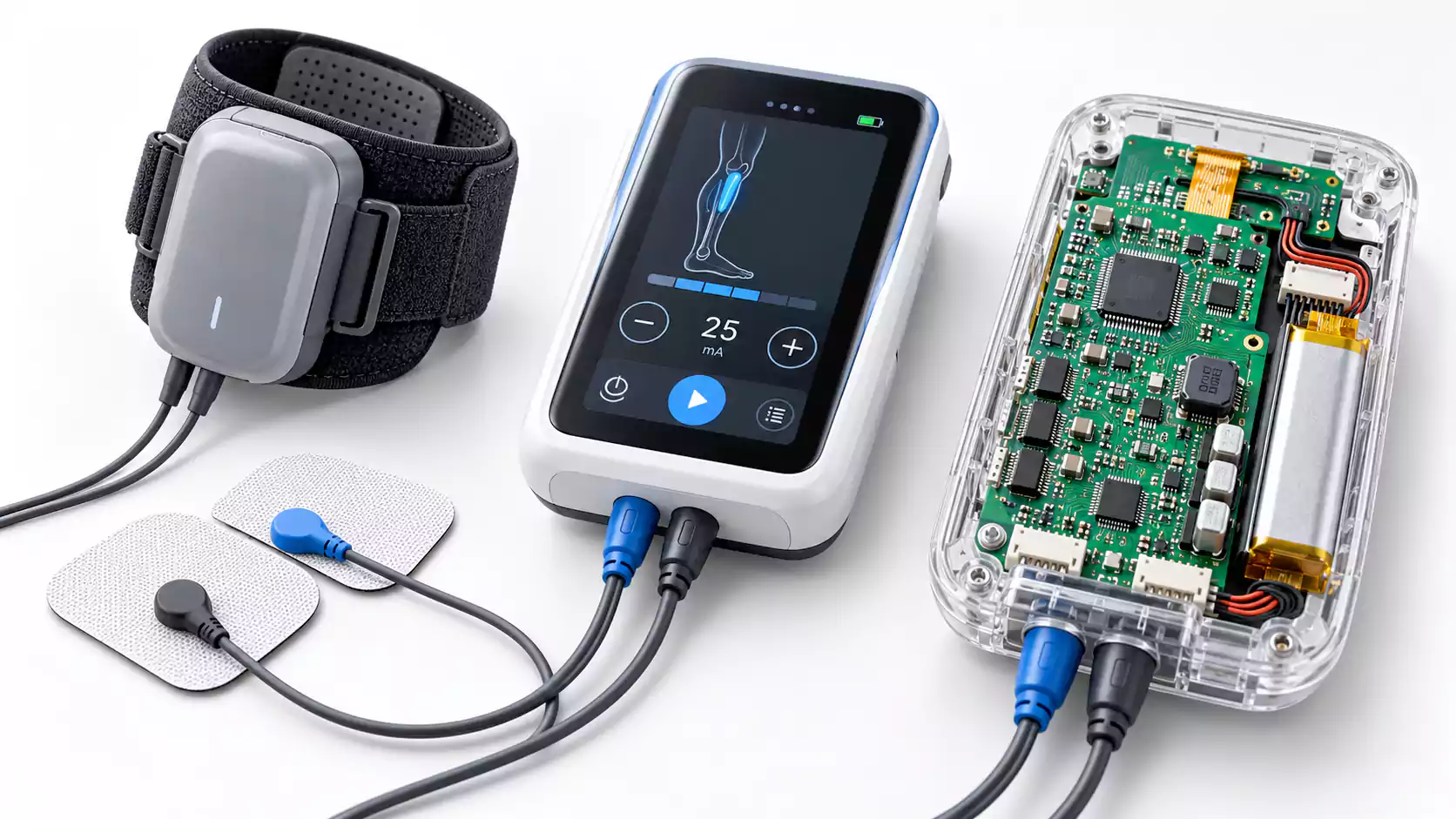

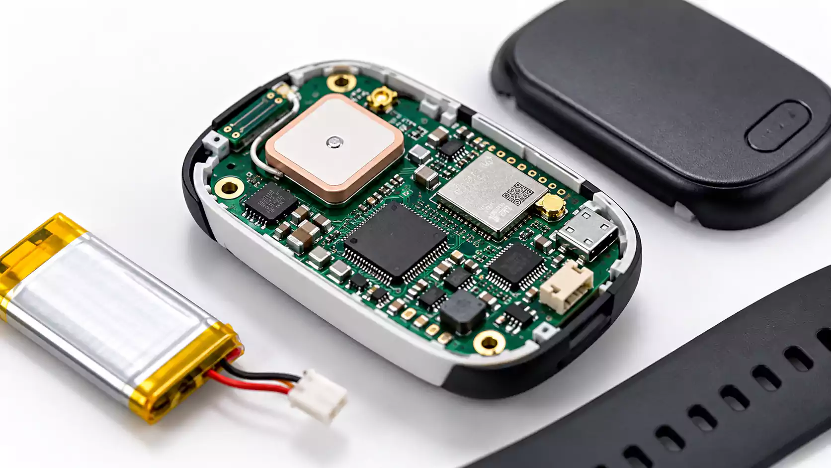

A reliable gas detector depends on the complete electronic signal chain.
On one compact board, the PCB may need to handle weak analog signals, heater current, switching power, digital processing, industrial interfaces, and environmental exposure.
A typical signal chain looks like this:
Gas Sensor → Analog Front End → Filter → ADC → MCU → Alarm / RS-485 / 4–20mA
Many designs also include DC/DC converters, heater drivers, relays, wireless radios, and 24V industrial inputs.
Effective Gas Detection PCB Design starts with the sensor technology and carries its requirements through the analog front end, power architecture, PCB layout, EMC protection, assembly process, and production testing.
Gas Sensor Technologies and Their PCB Requirements
Different gas-sensing technologies produce different electrical outputs and place different demands on the PCB.
| Sensor Type | Typical Signal | Main PCB Challenge |
| Electrochemical | nA to ?A current | TIA, leakage, high-impedance routing |
| MOS | Resistance change | Heater current, thermal drift |
| Catalytic bead | Bridge / mV signal | Stable excitation, low-level amplification |
| NDIR | Optical signal | IR drive, photodetector AFE, noise |
| Digital gas sensor | I?C / SPI | Power integrity, placement, airflow |
Electrochemical sensors often require very low-bias-current analog circuitry. MOS and catalytic sensors introduce heater power and thermal effects. NDIR systems combine optical emitters, detectors, and analog processing. Digital gas sensors integrate more signal processing inside the package while still depending on stable power and suitable physical placement.
A useful design principle is:
The gas sensor technology determines the PCB architecture.

Electrochemical Gas Sensor Front-End and TIA Layout
An electrochemical gas sensor PCB can be highly sensitive to leakage and noise because the sensor output may be only nanoamps or microamps.
A common signal path is:
Electrochemical Sensor → Potentiostat / TIA → Low-Pass Filter → ADC
A practical implementation can be found in Analog Devices' electrochemical gas measurement reference design, which supports 2-, 3-, and 4-electrode sensors and integrates sensor biasing, measurement, temperature/humidity sensing, and diagnostics.
The transimpedance amplifier converts sensor current into voltage:
VOUT = VBIAS ± (ISENSOR × RTIA)
Select the feedback resistance based on sensor sensitivity, maximum gas concentration, expected current range, and ADC full-scale input.
Keep High-Impedance Nodes Short
The connection between the sensor and amplifier input is usually one of the most sensitive parts of the gas sensor analog front end. TI's LMP91000 layout guidance similarly recommends keeping the RE, CE, and WE sensor traces short and separated from high-frequency signals such as clocks.
Short routing helps reduce capacitive pickup, leakage, and instability. Sensitive traces benefit from physical separation from DC/DC switching nodes, MCU clocks, fast digital buses, relay-drive signals, and heater current paths.

Control Surface Leakage
At nanoamp or microamp levels, small leakage paths can create measurable errors.
Common sources include:
- Flux residue
- Moisture
- Dust
- Connector contamination
- Ionic residues
Guard traces or guard rings can improve high-impedance performance in suitable areas. For a deeper look at PCB leakage current and guard-ring design, including contamination and high-impedance input behavior, see our related design guide.
For this reason, gas sensor TIA performance is closely linked to both circuit design and manufacturing quality.
Heater Power Isolation for MOS and Catalytic Sensors
MOS and catalytic gas sensors introduce a second major design challenge: heater power.
Heater current is much larger than the sensing signal. Shared copper paths can therefore create voltage drops that appear as measurement offset or noise.
A practical gas sensor heater circuit uses dedicated power and return paths.
Separate Heater Current From the Analog Path
Useful layout practices include:
- Route heater power separately from sensitive analog returns.
- Use sufficient copper width for heater current.
- Place local bulk and high-frequency decoupling near the heater supply.
- Keep heater-driver switching loops compact.
- Provide a direct heater return path that stays clear of the ADC and TIA area.
Treat Heat as a Measurement Variable
Heaters also create local temperature gradients.
A hot sensor or heater driver placed close to an ADC, voltage reference, analog front end, or temperature-compensation sensor can introduce drift.
Good heater isolation therefore considers both electrical coupling and thermal coupling.
Gas Sensor PCB Layout and Noise Control
A practical gas detector PCB layout becomes easier to control when the board is organized into functional regions.
A useful partition is:
- Sensor / AFE Zone
- ADC / Reference Zone
- MCU / Digital Zone
- Heater / Power Zone
- Industrial Interface Zone
The main objective is to keep sensitive current paths local and give noisy currents a short, predictable return path.
Keep Switching Power Away From Sensitive Analog Circuits
DC/DC converters are common in an industrial gas detection PCB, especially in systems powered from 12V or 24V rails.
Critical switching areas include:
- switching node
- inductor
- MOSFET or switching device
- input capacitor loop
Physical separation between these regions and the sensor input, TIA, ADC reference, and other high-impedance nodes helps reduce conducted and radiated noise.
A low-noise LDO can also follow a switching regulator when the AFE, ADC, or voltage reference needs a quieter rail.
Place the ADC and Reference Carefully
Keeping the ADC reasonably close to the analog front end helps shorten low-level analog routes.
Reference decoupling also benefits from compact placement. Move digital outputs directly toward the digital section to keep switching activity away from the measurement path.
Also consider input filtering alongside ADC settling time. An RC network can reduce unwanted noise while preserving sufficient settling for accurate conversion.
Sensor Placement, Airflow, and Thermal Effects
A gas detector relies on physical contact between the sensing element and the surrounding atmosphere. Sensor placement therefore affects both response time and measurement accuracy.
Important mechanical and thermal factors include:
- Enclosure vents
- Gas inlet position
- PCB edge location
- Dust filters or membranes
- Nearby batteries
- Power converters
- Heater drivers
- Other heat-producing components
Placing the sensor in a clear airflow path improves exposure to the target gas.
Thermal separation also matters. Local heating from regulators, batteries, and heater circuitry can influence sensor response or distort temperature and humidity compensation.
In practice, the PCB and enclosure form one sensing system.
Industrial Interfaces and EMC Protection
Gas detectors used in factories, process equipment, mining, environmental monitoring, and building safety often connect to long external cables. These installations introduce many of the same protection and grounding challenges found in long sensor cable PCB design, including common-mode noise, ground-potential differences, ESD, EFT, and surge exposure.
These cables can carry ESD, EFT, surge energy, and common-mode noise directly into the electronics.
Effective protection begins at the cable entry.
24V Power Inputs
A typical industrial input may include:
- Reverse-polarity protection
- TVS protection
- Input filtering
- Surge protection
Locating transient protection near the connector helps keep high-energy disturbances away from the rest of the board.
RS-485 and 4–20mA Interfaces
RS-485 is widely used for digital industrial communication, while 4–20mA remains common in process instrumentation. For current-loop receiver circuits, our guide to 4–20mA analog input PCB design covers shunt selection, protection, filtering, isolation, and ADC interfacing in more detail.
PCB design should account for:
- Termination
- TVS protection
- Common-mode disturbances
- Isolation where required
- Cable shield termination
- Ground-potential differences
Relay and alarm outputs also require careful current-return planning because inductive loads can introduce additional switching noise.
Cleaning, Conformal Coating, and Gas Sensor Assembly
Gas sensors often have assembly requirements that differ from standard SMT components.
Depending on the device, the manufacturing process may need to account for:
- Reflow temperature
- Board washing
- Ultrasonic cleaning
- Solvent exposure
- Storage conditions
- Conformal coating
The sensor manufacturer’s handling and assembly specifications should therefore be included in the PCBA process plan.
Conformal Coating Requires Selective Masking
Coating chemistry and environmental resistance also vary by application; our guide to conformal coating for PCBs compares common coating types, protection benefits, and application considerations.
Areas that may require masking include:
- Gas inlet
- Sensing membrane
- Optical window
- Removable sensor socket
- Calibration access
- Selected connectors
The practical objective is:
Protect the electronics while keeping the sensing element fully exposed to the intended environment.
PCB Cleanliness Matters
Low-current analog circuits are especially sensitive to contamination.
Flux residue or ionic contamination around the TIA, sensor connector, or other high-impedance nodes can create leakage paths and measurement drift.
A well-controlled gas detector PCBA process therefore needs a cleaning strategy that matches both the analog requirements and the sensor manufacturer’s restrictions.
Gas Detection PCB Testing and Calibration
Manufacturing inspection verifies assembly quality, while functional testing and calibration verify the electrical and sensing performance.
Different test stages serve different purposes.
| Test | What It Verifies |
| AOI / X-Ray | Assembly quality |
| Electrical FCT | Power rails, MCU, communication |
| Analog-path test | TIA, amplifier, filter, ADC |
| Heater test | Heater voltage and current |
| Sensor simulation | Measurement signal chain |
| Zero / span calibration | Sensor and system response |
| Known-gas test | Complete detector performance |
A production fixture can verify the AFE, ADC, MCU, heater, alarm, and communication interfaces.
Final gas concentration accuracy may also depend on:
- Sensor sensitivity
- Sensor lot variation
- Temperature
- Humidity
- Zero/span calibration
- Known-gas verification
Accessible test points and connectors make the analog and digital signal chains easier to verify during production.
Gas Detection PCB Design Checklist and Common Failure Modes
Before releasing a gas detector board for production, review the following points.
| Design Check | Potential Issue |
| Keep the AFE close to the sensor | Noise pickup and instability |
| Minimize high-impedance trace length | Leakage and interference |
| Provide a dedicated heater return | Measurement drift |
| Separate DC/DC circuitry from the AFE | Switching noise |
| Protect external cable entries | ESD, EFT, and surge failures |
| Maintain a clear airflow path | Slow or inaccurate response |
| Mask the sensor during coating | Sensor contamination |
| Control PCB cleanliness | TIA leakage |
| Provide production test access | Difficult diagnosis |
| Plan FCT and calibration separately | Functional hardware with poor measurement accuracy |
Successful Gas Detection PCB Design brings the sensor interface, analog front end, heater power, PCB layout, airflow, EMC protection, assembly process, and production testing into one coordinated design.
Careful attention to these areas helps reduce noise, measurement drift, environmental failures, and production-to-production variation as a gas detector moves from prototype to volume manufacturing.
For industrial gas detection and sensor electronics, MULTIPCB provides PCB fabrication, component sourcing, PCB assembly services, DFM review, and production testing from prototype builds through volume production.
