




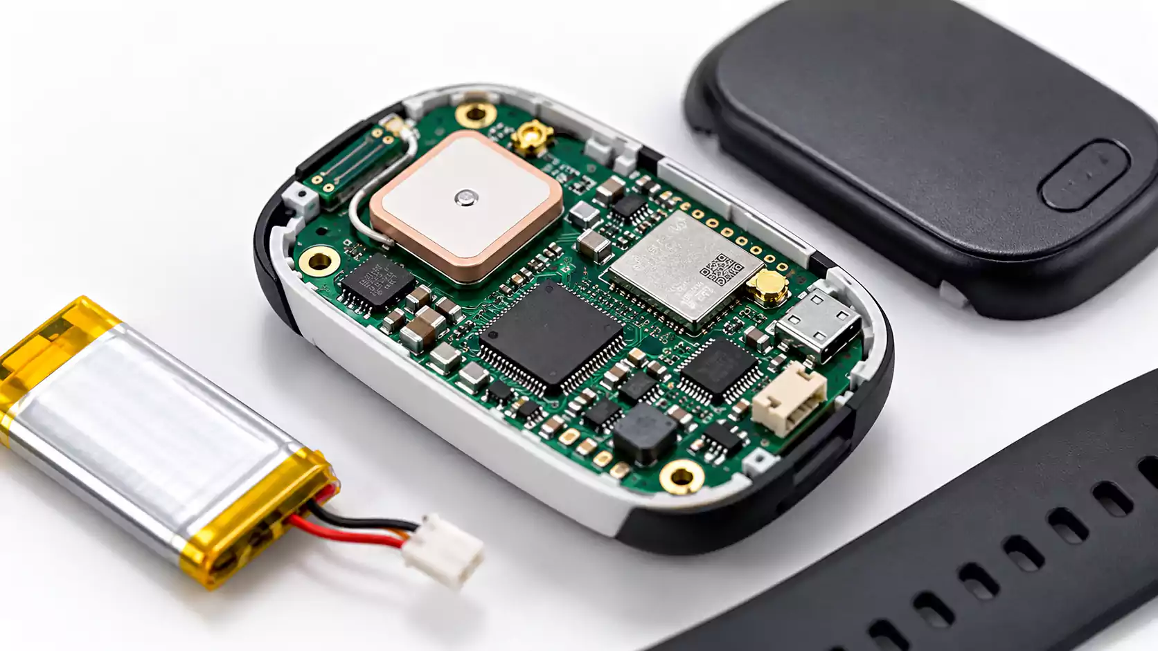

A load cell PCB is a precision analog interface that powers a strain-gauge bridge, conditions its millivolt-level differential output, and converts the signal into calibrated force or weight data.
The main challenge is the very small signal level. For example, a load cell rated at 2 mV/V with 5 V excitation produces only:
at full scale.
At lower loads, the signal is smaller still. Amplifier offset, excitation noise, thermal drift, cable interference, reference instability, and PCB layout can therefore directly affect measurement accuracy.
Key design rule: A 24-bit ADC cannot recover accuracy already lost in the analog front end, excitation path, PCB layout, or calibration process.
A typical signal chain is:
Load Cell → Protection & Filtering → AFE/PGA → 24-Bit ADC → MCU

Load Cell PCB Signal Chain and Front-End Architecture
Most strain-gauge load cells use a Wheatstone bridge and specify output sensitivity in mV/V. The PCB must preserve this small differential signal while rejecting common-mode noise and power-supply interference.
A typical Load Cell PCB Design includes the following functional blocks:
| Bridge excitation | Powers the strain-gauge bridge | Noise and drift |
| Input protection | Protects external sensor inputs | Leakage and capacitance |
| Analog filtering | Suppresses EMI and aliasing | Input imbalance |
| INA / PGA | Amplifies the bridge output | Offset and 1/f noise |
| 24-bit ADC | Converts analog signal to digital data | Input-referred noise |
| MCU | Calibration and processing | Digital noise coupling |
Instrumentation Amplifier vs. Integrated PGA ADC
There are two common architectures.
Instrumentation amplifier + ADC
This gives the designer more control over gain, filtering, common-mode range, and ADC selection. It is useful when a custom Strain Gauge Amplifier Circuit is required.
Integrated PGA + ADC
A precision sigma-delta ADC may integrate the programmable gain amplifier, differential input stage, digital filter, and reference interface. This can reduce BOM size and simplify a compact Load Cell Amplifier PCB.
| INA + ADC | Flexible gain and filtering | More components and board area |
| PGA + ADC | Compact and simpler BOM | Less analog flexibility |
| Dedicated load-cell ADC | Easy integration | Device-specific limitations |
The correct choice depends on required accuracy, bandwidth, temperature stability, and production cost.
4-Wire vs. 6-Wire Load Cell Interface Design
The choice between a 4-wire and 6-wire load cell affects both the interface circuit and PCB routing.
4-Wire Load Cell
A standard 4-wire load cell uses:
- Excitation+
- Excitation?
- Signal+
- Signal?
This arrangement is simple and works well when cable resistance is low enough that excitation voltage drop does not significantly affect accuracy.
6-Wire Load Cell
A 6-wire load cell adds:
- Sense+
- Sense?
These sense lines monitor the actual excitation voltage at the bridge. This helps compensate for voltage drop along the cable, which can otherwise introduce gain error in high-accuracy or long-cable applications.
| Design Factor | 4-Wire | 6-Wire |
|---|---|---|
| Wiring complexity | Lower | Higher |
| Remote sensing | No | Yes |
| Cable-drop compensation | Limited | Better |
| Long-cable accuracy | Moderate | Better |
| Precision applications | Common | Often preferred |
For a 6-wire Load Cell Interface PCB, route the sense lines as precision analog signals and keep them away from switching nodes, power traces, and noisy digital circuitry.
Excitation, Reference & Ratiometric Architecture
Bridge excitation and ADC reference should be designed as part of the same measurement path.
Why Ratiometric Measurement Matters
A load cell’s output is proportional to its excitation voltage:
The ADC code depends on the ratio between the input signal and the reference voltage:
If the ADC reference tracks the bridge excitation:
then much of the common excitation variation cancels.
This is the principle behind Load Cell Ratiometric Measurement. Rather than relying only on an extremely stable excitation source, the design makes the ADC reference follow the same voltage that drives the bridge.

6-Wire Load Cells
In a precision 6-wire system, the ADC reference should ideally reflect the actual excitation voltage at the load cell, not just the nominal voltage generated on the PCB.
The Sense+ and Sense? lines help account for voltage drop in long cables, improving measurement accuracy.
Noise Budget and 24-Bit ADC Selection
A 24-bit ADC for Load Cell applications does not mean the system will deliver 24 bits of usable resolution.
If the full-scale bridge output is 10 mV:
This is only a theoretical code width. In practice, the measurement is limited by the total noise of the bridge, analog front end, ADC, reference, PCB, and surrounding environment.
Input-Referred Noise Budget
A simplified noise model is:
The main contributors typically include:
- Bridge thermal noise
- Amplifier input noise
- ADC input-referred noise
- Excitation and reference noise
- PCB-coupled interference
- External EMI
For Load Cell ADC PCB Design, focus on input-referred noise, noise-free resolution, PGA gain, 50/60 Hz rejection, sampling rate, common-mode range, and reference configuration. Static weighing systems typically prioritize low noise and line-frequency rejection, while dynamic force measurement requires more bandwidth and a different noise-performance trade-off.
For more detail on reference routing, grounding, and noise control, see our 24-bit ADC PCB layout guide.
Input Protection, Filtering and Long-Cable EMI Control
The load-cell connector is an external entry point, so protection should be placed before the sensitive analog front end. Common protection components include:
- TVS diodes
- Series resistors
- EMI filters
- ESD protection devices
For precision inputs, selection should also consider leakage current, parasitic capacitance, added series resistance, and matching between the differential paths.
Differential Filtering
A balanced RC filter helps reduce differential and common-mode interference. Both input paths should remain closely matched to preserve common-mode rejection.
Long Load Cell Cables
Long sensor cables can pick up:
- 50/60 Hz mains noise
- Motor and VFD interference
- Relay transients
- Ground-potential differences
Effective Load Cell Noise Reduction usually combines twisted-pair or shielded cabling, balanced filtering, proper chassis grounding, and a high-CMRR analog front end. For longer sensor connections, see our guide to long sensor cable PCB design for protection, shielding, and filtering considerations.
Precision Load Cell PCB Layout & Stackup Rules
The Load Cell PCB Layout should create a compact, quiet measurement zone around the connector, filter, amplifier, ADC, and reference.
Recommended 4-Layer Structure
| L1 | Load-cell input, AFE, ADC, precision analog |
| L2 | Continuous GND plane |
| L3 | Power distribution |
| L4 | MCU and secondary signals |
A continuous PCB ground plane gives sensitive analog signals a predictable return path and helps control noise coupling.
6-Layer Option
For boards that also include USB, Ethernet, CAN, wireless, or multiple power rails:
| L1 | Sensitive analog + components |
| L2 | Solid GND |
| L3 | Power |
| L4 | Digital routing |
| L5 | Solid GND |
| L6 | Secondary signals/components |
The exact stackup should still be coordinated with the PCB manufacturer.

Critical Layout Rules
For a low-noise Load Cell PCB Layout, keep the load-cell connector, AFE, and ADC close together, route bridge inputs short and symmetrical, and keep switching power circuits and fast digital signals away from the analog section.
Precision Components & Thermal Drift Management
Load-cell accuracy depends not only on noise, but also on temperature stability. Resistor tolerance alone is not enough; several parameters affect long-term measurement accuracy:
- Tolerance
- TCR
- Resistor matching
- Tracking TCR
- Long-term stability
Matched resistor networks are often preferred in gain-setting or bridge-completion circuits because their elements can track temperature more consistently than separate discrete resistors.
Thermal drift can also come from the amplifier, ADC reference, and nearby heat sources. Keep precision analog components away from DC/DC converters, power MOSFETs, regulators, and other hot devices.
At very small signal levels, PCB temperature gradients can introduce thermoelectric offsets. For precision measurement, electrical symmetry and thermal symmetry should be considered together.
Load Cell Calibration Techniques
Calibration is necessary even when the analog design is excellent.
Zero Calibration
Measures unloaded offset and removes the system zero error.
Span Calibration
Uses a known load to determine system gain.
Multi-Point Calibration
Can improve linearity in higher-accuracy systems.
Temperature Compensation
May be required when the system operates across a wide temperature range.
Load Cell Shunt Calibration
Load Cell Shunt Calibration uses a precision resistor to create a known imbalance in the Wheatstone bridge.
This allows the system to verify the complete signal chain:
Bridge → Cable → Connector → AFE → ADC → Firmware
A production design may use a precision shunt resistor with an analog switch or MCU-controlled path to automate calibration. This makes shunt calibration useful during production testing, commissioning, and maintenance.
From Load Cell PCB Design to PCBA Production and Testing
A precision analog design must remain consistent through PCB assembly and production. Key controls include precision resistor TCR, matched resistor networks, ADC/reference selection, and stable component sourcing.
AOI and continuity testing cannot verify analog accuracy, so functional testing should check the measurement path directly.
| Test | Purpose |
|---|---|
| Bridge excitation | Verify excitation accuracy |
| Zero-input reading | Check offset |
| Known differential input | Verify gain |
| ADC noise test | Check stability |
| Shunt calibration | Verify the signal chain |
For volume production, shunt calibration can be integrated into automated functional testing:
Zero → Apply Shunt → Measure ADC Code → Compare Limits
FAQ
What is the difference between a 4-wire and 6-wire load cell?
A 4-wire load cell uses excitation and signal pairs. A 6-wire load cell adds remote-sense lines to compensate for excitation voltage drop, especially over long cables.
Why is ratiometric measurement important for load cells?
Load-cell output varies with excitation voltage. Using a reference that tracks the bridge excitation helps cancel common excitation changes and improve measurement stability.
What is load cell shunt calibration?
Shunt calibration applies a precision resistor to create a known bridge imbalance, allowing the complete measurement chain to be checked without applying a physical load.
Should AGND and DGND be split on a load cell PCB?
Usually not. A continuous ground plane with controlled return paths is generally more predictable. Follow the ADC datasheet and actual current paths when defining the grounding strategy.
Conclusion
Reliable Load Cell PCB Design requires much more than placing a strain-gauge amplifier beside a 24-bit ADC. Excitation and reference architecture, noise budget, cable interface, PCB stackup, thermal drift, component matching, calibration, and production testing all influence final measurement accuracy.
For industrial weighing systems, force sensors, robotics, and precision instrumentation, MULTIPCB can support PCB fabrication, component sourcing, PCBA assembly, DFM review, and functional-test planning from prototype through production.
